Menu
Loadline Design
The output of a power amplifier (PA) is terminated with a specific impedance. This impedance is required for optimal linearity or power generation or efficiency or combination of such specs, and is determined by loadpull analysis. We call it loadline. While a loadline helps PA deliver its performance, the matching (VSWR) gets ruined because we do not present conjugate load to PA. Typically, we insert a circulator between antenna and PA such that reflections don’t reach back to PA, and get absorbed in port 3 of circulator as shown in image below.
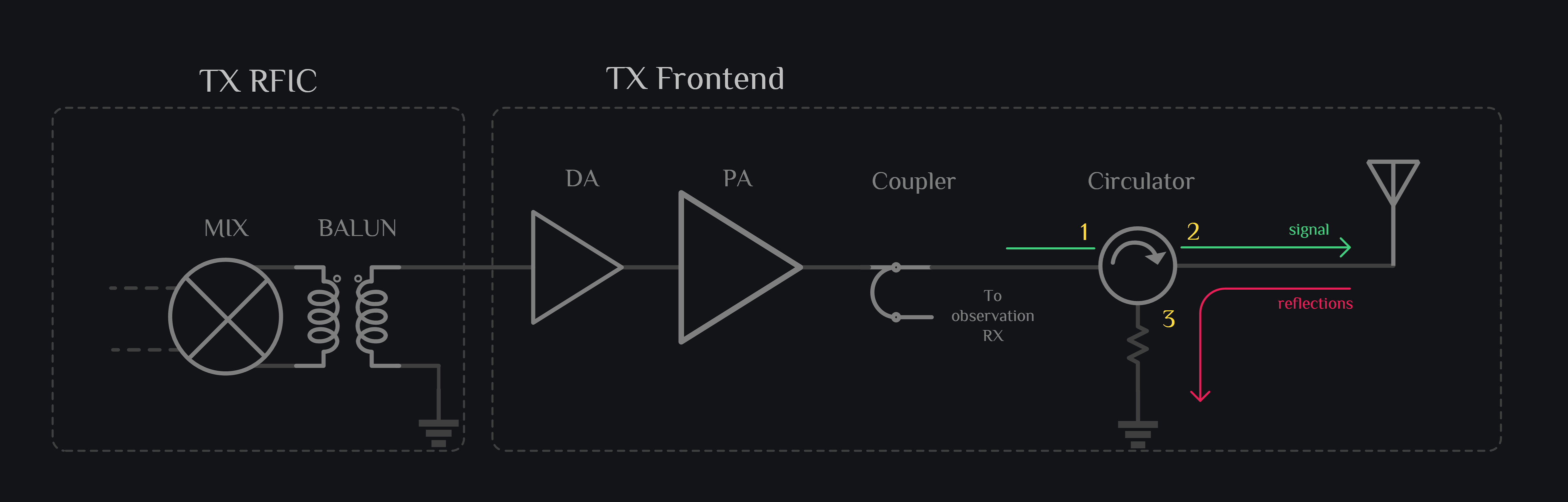
This works fine for front-end modules where off-the-shelves blocks can be patched together to curb the ailment. In context of TX RFIC where adding an circulator might not be possible (as they are made of ferrite), we discuss how loadline can be designed while also meeting the VSWR requirements.
Problem Statement
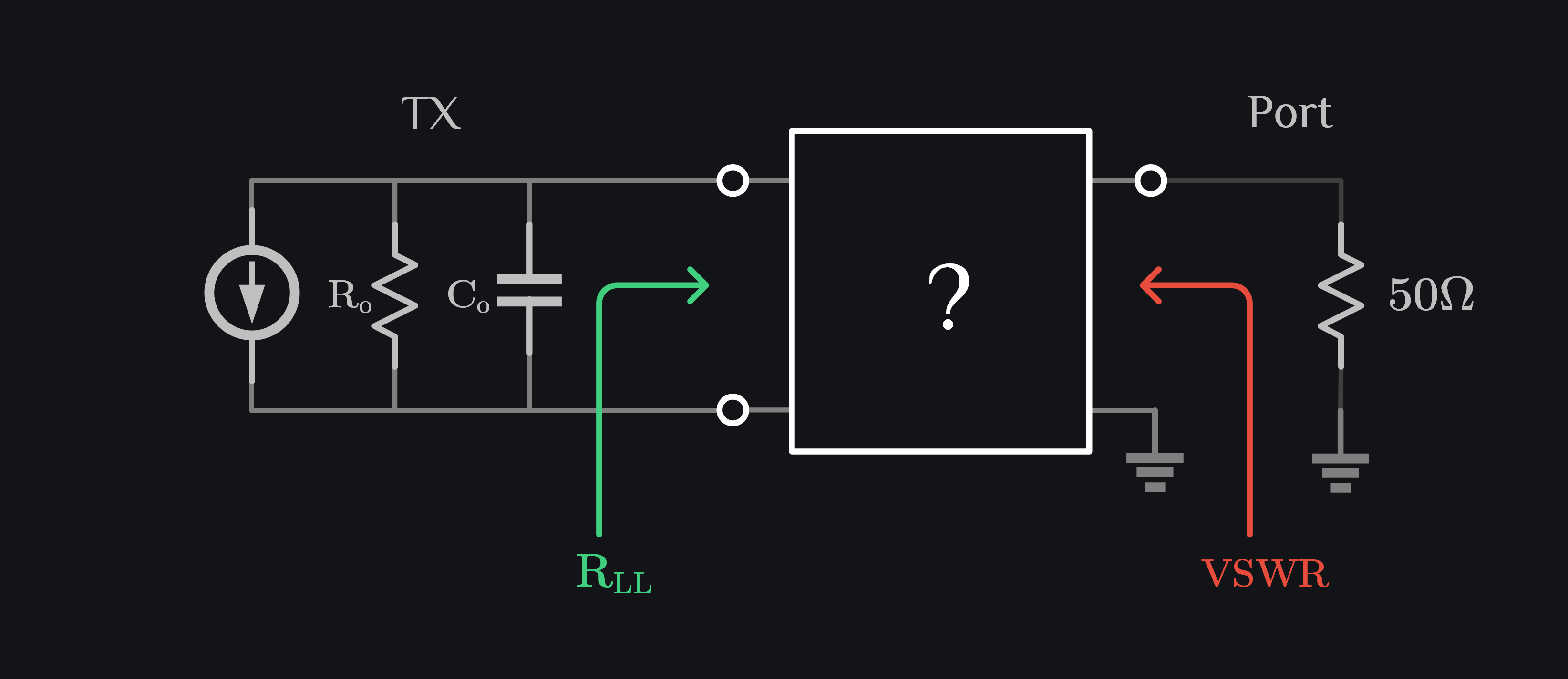
Say we have a TX with output resistance Ro and output capacitance Co. We have a requirement to present a certain resistance RLL to this TX, and also maintain certain VSWR looking from 50\(\Omega\) port. TX is differential, so we also want to convert it to single ended while doing so. Our job is to figure out how should the white box be designed.
Solution
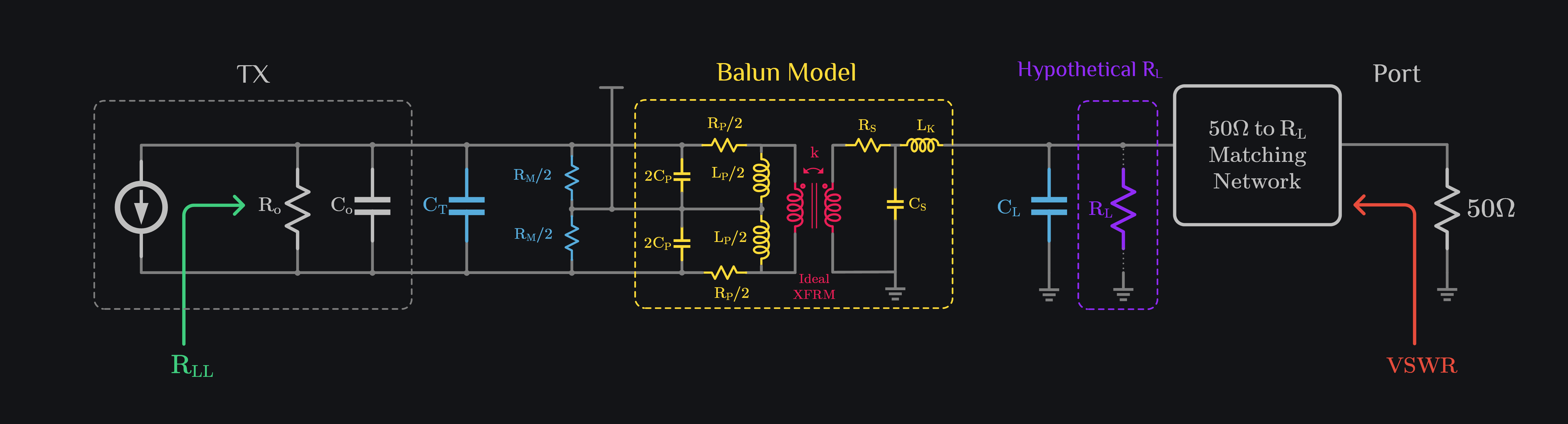
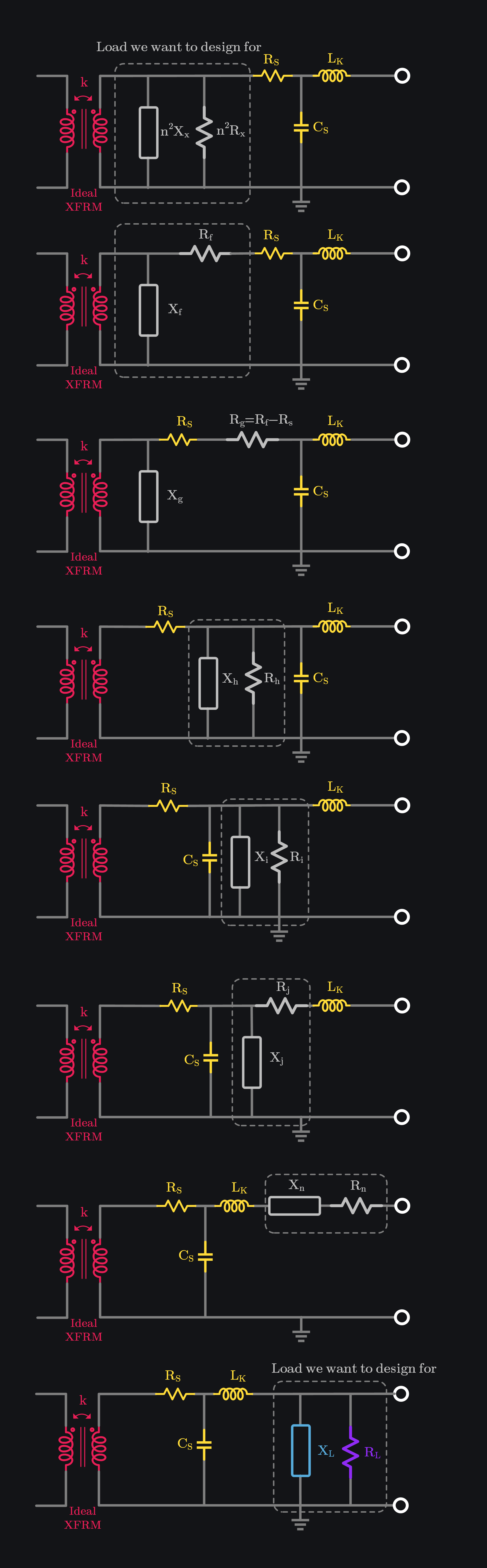
One of the ways we can accomplish this is shown in image below. First, we add a balun to convert differential to single ended. Second, we add a resistor RM to introduce loss into system as we will see later that simultaneous RLL and VSWR requirements cannot be satisfied without adding RM (also see a note on similar topic in appendix). We also add a capacitor CT at primary of balun to tune out primary inductance partially, and CL at secondary to tune out leftover inductance. (We mentioned tuning out primary inductance but not secondary – because there is only one inductance to tune out, the other inductance is a leakage inductance LK which is very small or zero if coupling coefficient is one, see transformer model # 4). One can just use CT or CL to tune out, we distributed the cap because it gives us a knob for loss optimization (more on this later). Our goal is to find RL and CL such that both RLL and VSWR are satisfied. Note RL is not a physical resistor, it the resistance value to which we want our 50\(\Omega\) port to convert to.
Loadline Design
Primary Side Calculations
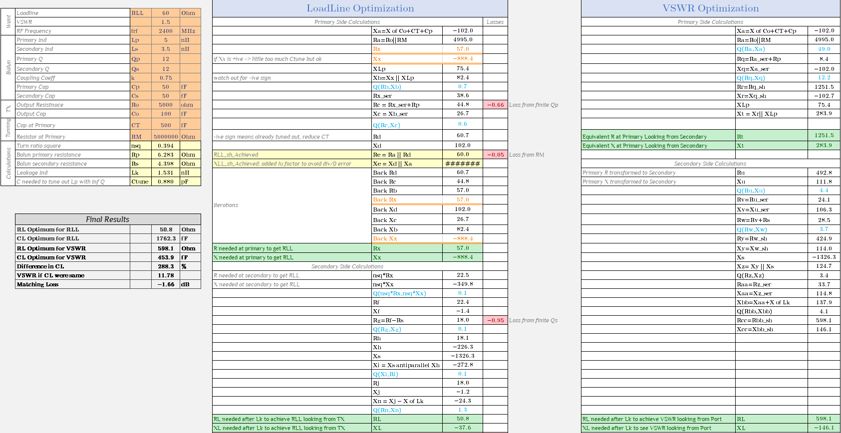
Let’s put some numbers in. Say we have 5k\(\Omega\) Ro and 100fF Co. We have CT, RM, Lp, Ls, k, Qp, Qs at our disposal to optimize. We start with 5nH Lp. It’s just a guess, you can use any Lp, things you would need to consider in choosing Lp are:
- how much Qp are you getting (the higher the better)
- what is the self-resonance frequency (the higher the better)
- how much area it takes (the lower the better)
- tuning capability (a higher Lp would need small tuning cap, which makes design very sensitive to parasitic and process variations)
- how much k you get (the higher the better)
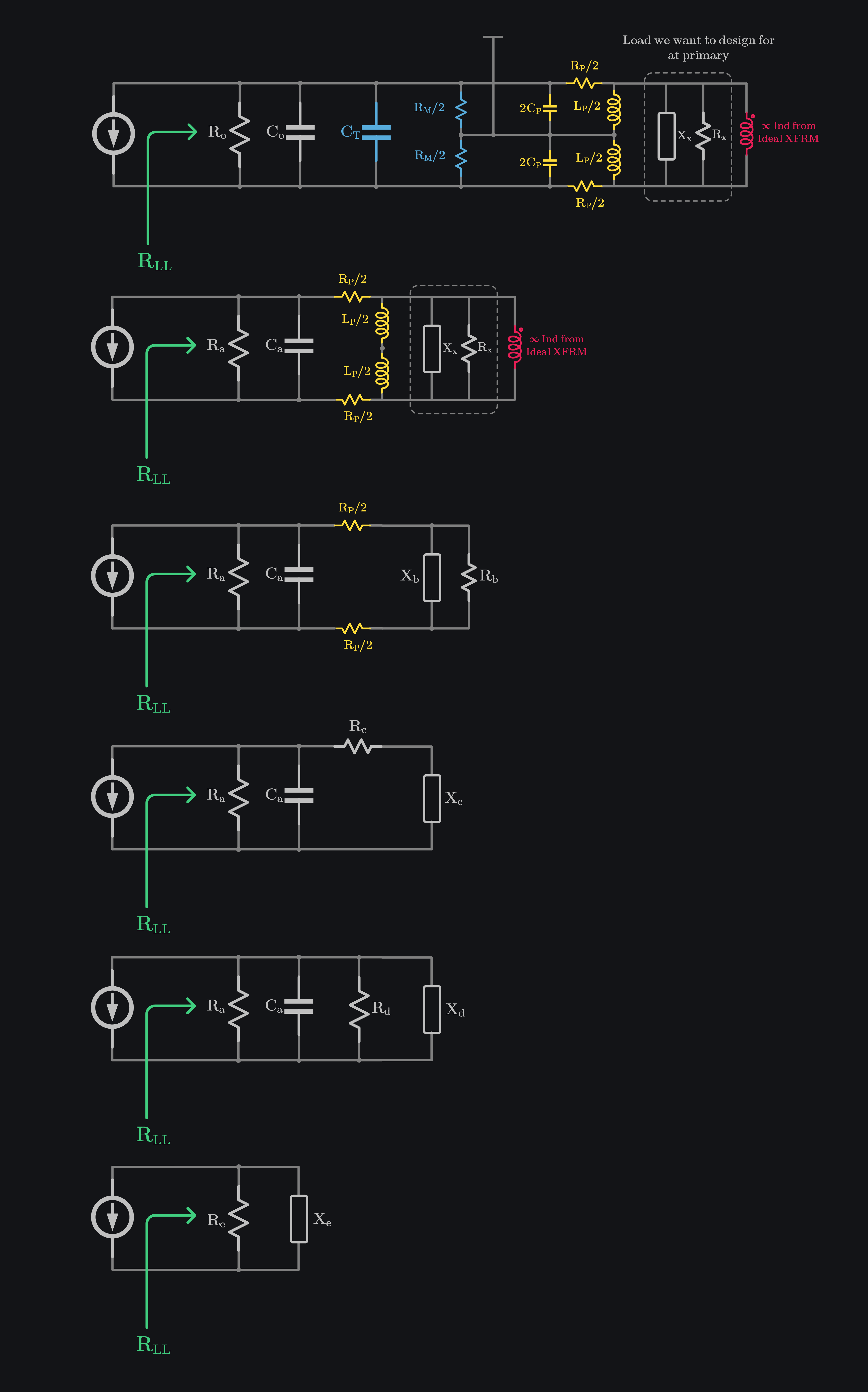
Ls is usually chosen to be 0.707 or 1.414 of Lp because this aspect ratio usually gives the highest k. Let’s make RM infinite for now, and choose a random value of CT, and begin! First, let us find what values of resistance and reactance do we need looking into primary of balun, that would get us desired loadline. Let’s call them Rx and Xx. We believe an analytical solution maybe worked out but we went with iterative solution in Microsoft Excel. We assume some initial value of Rx and Cx, and start simplifying the circuit till we get to Re and Xe. This is shown in image to the right starting from top and ending at bottom. Excel would keep iterating different values of Rx and Xx until it gets us \(R_e=R_{LL}\) and \(X_e=\infty\), which is what we would want to see pure RLL.
Secondary Side Calculations
Once we have found Rx and Xx needed at primary, we can multiply it by turn ratio square and figure out an equivalent RX needed at secondary. We then move this RX step by step towards the output, and finally arrive at RL and CL values. Basically this would mean: attach a CL capacitor at output node, and attach a matching network that transforms port 50\(\Omega\) to RL. If done, your RL CL would transform through balun parasitics and other components we added, and once they make it to TX current source, all the imaginary part would have been stripped off and you should see real RLL.
(Note it is also possible that your matching network transforms port 50\(\Omega\) to RL || XL directly, so one can remove CL)
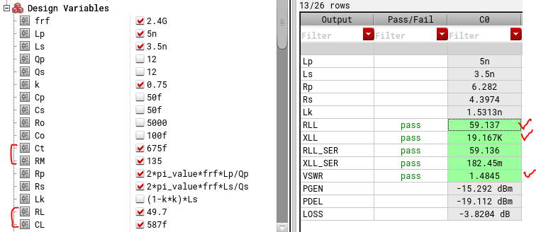
We built an Excel calculator which details these calculations. Different parameters we assumed are in oranges boxes and RL CL values under Final Results. Our goal was 60\(\Omega\) RLL, and our calculator says we need to have \(R_L=50.8\Omega\) and \(C_L=1762.3fF\) to achieve this RLL. Ok great, how about VSWR though? Our Excel sheet does similar calculations for VSWR and shows that we need \(R_L=598.1\Omega\) and \(C_L=453.9fF\) to get 1:1 VSWR. This RL CL is way way off from what we need for RLL. This is not surprising as VSWR is simplify looking for conjugate load which happens to be very different from our desired RLL. In other words, if we had just gone for conjugate match for TX output, our VSWR would have been perfect but we would not have gotten the RLL we wanted.
Simultaneous Loadline and VSWR Optimization
How can we remedy this situation where we have different RL CL values to meet given RLL and VSWR? By adding RM. See that our loss in image above is 1.66dB, once we add RM we can tradeoff loss with VSWR. Let’s set our VSWR target to 1:1.5. By playing with RM and CT (of course you can play with other variables too, everything is on the table) we can arrive at RL CL values which will give the RLL we want while meeting the VSWR. Image below shows that we don’t need different value of CL now, and RL are still somewhat different but they meet VSWR condition. You can make RL values similar too by reducing RM at the expense of more loss. We are already hitting 3.86dB loss to get 1.5 VSWR. Our finally RL and CL are 49.7\(\Omega\) and 587fF.
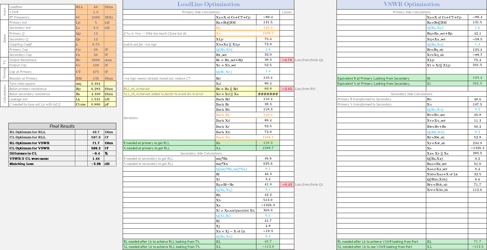
Now one might ask that role of RM is clear, but what do we need CT for. Can we get rid of CT and just use CL to tune out balun? The answer is yes but at the expense of slightly higher loss (not always though, devil lies in details, one need to analyze the particular situation). CT was placed strategically. Ideally, we should tune out things where they emerge, meaning we should have tuned Lp right where it was (at primary). If we don’t tune it here, and instead try to get the -ive reactive part all the way from CL, it will go through impedance transformations at different nodes (as shown in images above) and at some node if Q is high, it will result in higher loss. How do you know at which node Q is high? You can lookup the Q of all the nodes in our Excel calculator, it’s colored sky blue.
Another question one might ask is if loss gets us VSWR, can we get rid of RM and instead make our balun intentionally lossy (i.e., lower Q)? The answer is not really. It turns out series and shunt losses are different. A series resistor creates two nodes in the circuit and hence creates asymmetry in left and right impedances. For example, if you see that optimum of VSWR and RLL don’t align in frequency that is maybe you got optimum RLL at 2.4GHz but optimum VSWR at 2.5GHz, know that this is because of series resistor somewhere. A shunt resistor keeps this symmetry. Since inductor’s loss is physically a series resistor, we always want to maximize Q to reduce this resistor. Also there are other benefits of putting RM (as shown in our circuit, center of RM goes to supply, we intentionally made it a common mode), this helps in providing even harmonics a path to ground. Otherwise, they will be forced to find a way to circulate in your circuit and create non-linearities you wouldn’t have imagined (like weird combinations of mixing products with your signal, that will land back at your IM3s/5s for example).
Loadline Design Verification in Cadence
Let’s now head to Cadence and plug our numbers in to see if our methodology works. Cadence schematic is shown below. Note that there is no explicit LK here because that was just for our math, real LK is modelled by finite k which we have added in our circuit using “mind” instance in analogLib. Also note that there are two circuits shown but they are exactly the same, just different excitations: one measures RLL and other measures VSWR.
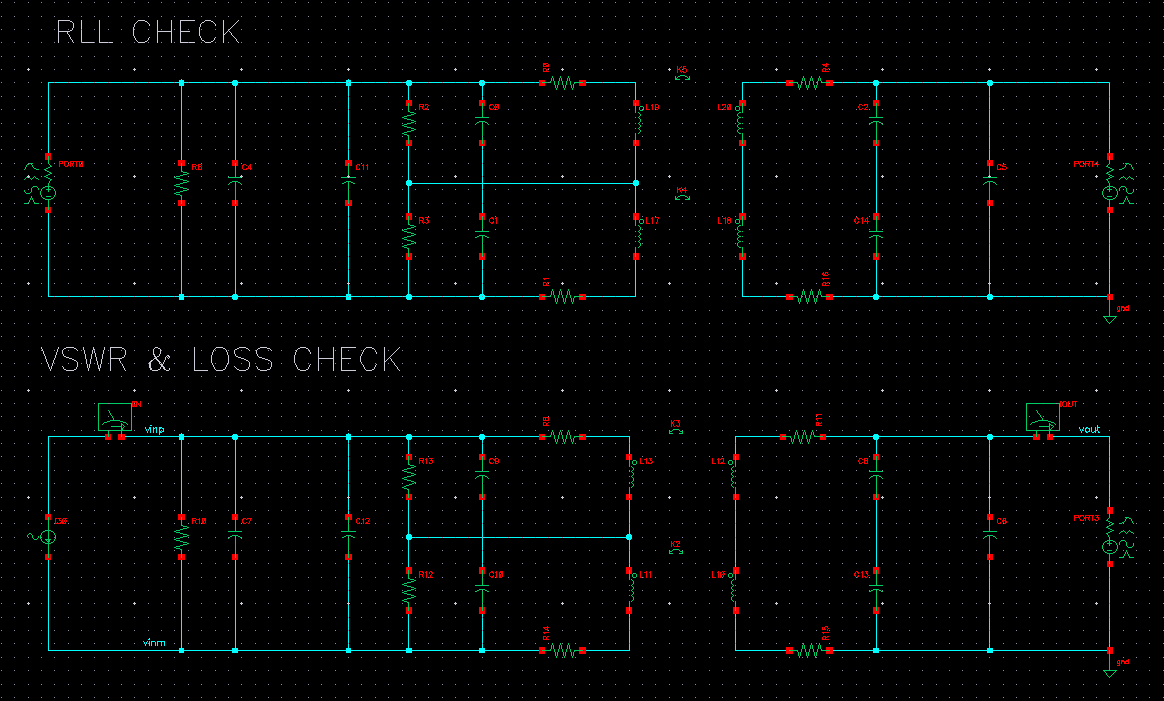
Image below shows simulation results. Our target was 60\(\Omega\) RLL and 1:1.5 VSWR. RLL, VSWR and loss are match pretty well with our calculations.
Excel calculator is attached below. One can start with this calculator to gain insights into circuit (like where is loss coming from, what variable does what, and which variable needs tight control in terms of design sensitivity) and later move on to directly optimize in Cadence.
Appendix
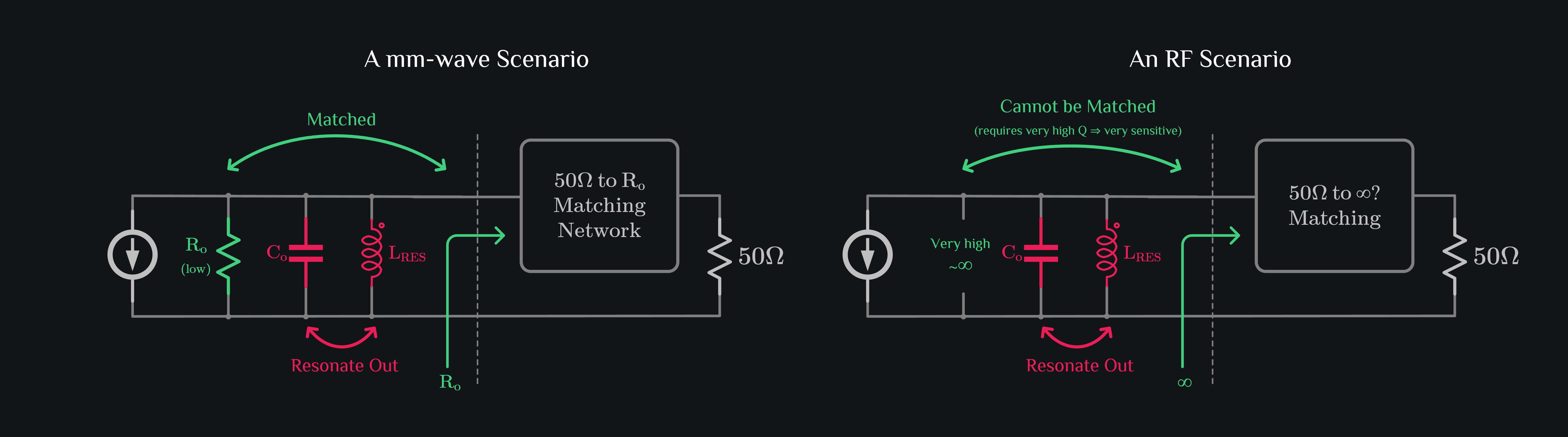
A subtle difference between mm-wave and RF impedance matching: at mm-wave, transistor output already contains low resistive part (either with existing losses in the circuit or through numerous feedback paths between output and different nodes of circuit that eventually introduce real part in output impedance), therefore one can just go on matching port to transistor output impedance. At RF, real part of output impedance is quite high (almost an open circuit) making it impossible to match to 50\(\Omega\\) because matching network requires very high Q which makes matching very sensitive and low bandwidth. Therefore, we intentionally add a resistor to introduce real part, making things low Q and match-worthy.
(One can think of ways of adding a real part to transistor output impedance without adding resistor itself and that would work too)
Browse by Tags
aclr (3)
ADS (1)
amplifier (1)
balun (2)
bandwidth (1)
cadence (8)
concept (1)
design (1)
device (8)
EM (1)
evm (1)
fft (1)
ideal (1)
ideal low pass filter (2)
inductor (2)
intermodulation (4)
IQ calibration (1)
linearity (13)
loadline (1)
LO leakage (1)
matching network (8)
math (6)
mixer (5)
mmwave (1)
noise (3)
product (1)
quality factor (7)
specs (2)
transformer (1)
tx (17)
verilog (1)
RFInsights
Published: 14 Jun 2023
Last Edit: 14 Jun 2023