Short story: Conjugate match transfers maximum power whereas loadline match generates maximum power.
Long story: You know this already that maximum power is transferred when you do conjugate matching, and yet when we talk about power amplifiers we have the audacity to say we will be matching to a specific impedance called as loadline. If you do conjugate matching for power amplifier, you won’t get maximum output power at all. Period. Okay, but nobody tells you that its not just about maximum power transfer, it is about maximum power generation as well. And your conjugate load may not let the transistor generate maximum power.
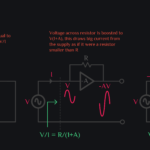
Assume you have a big output transistor for power amplifier, its output impedance is very low (say Rlow || C). You conjugate load will say, ok present Ltune || Rlow where Ltune is set to resonate out C, then you would be all set and have maximum power transfer. However, load that your PA will see now is very small (0.5Rlow), and voltage swings generated across transistor will also be very small, thus underutilizing the transistor and not generating max power at all. Similarly, if your PA had high output impedance (say Rhigh || C), your conjugate load will be Ltune || Rhigh, your PA would see a much bigger impedance (0.5Rhigh), it can generate huge voltage but now the current drawn by the load would be too small, again limiting your power generation.
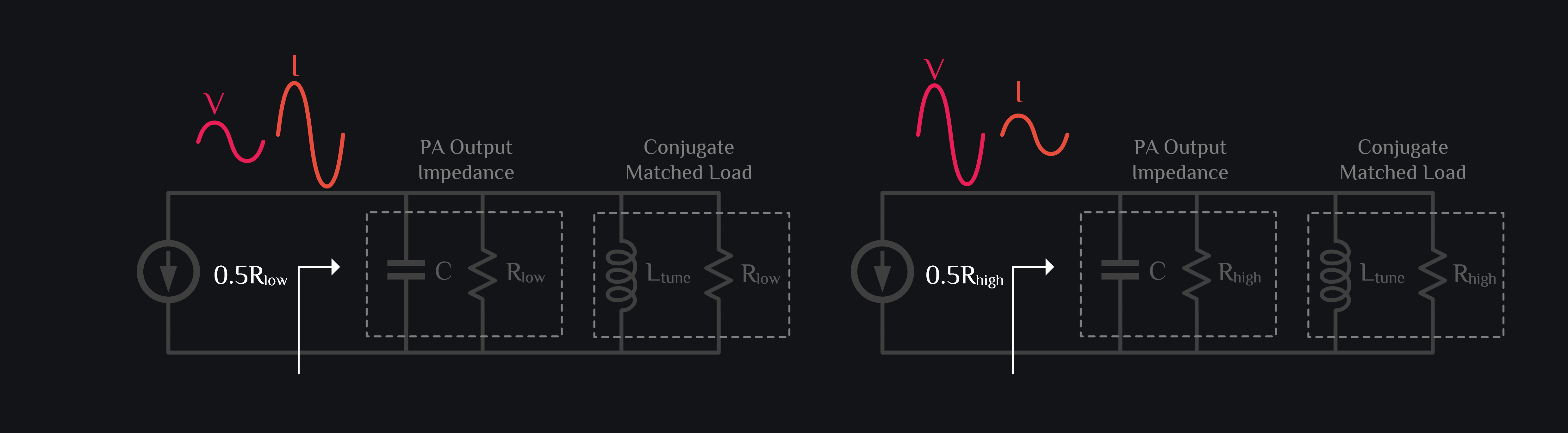
So, how do you find a load that extracts maximum power from transistor? Optimum load for maximum power generation from the transistor is simply R = Vmax/Imax.
For example, for device biased in class-A, you can give optimal load as:
Ropt = (Vhigh – Vlow) / Imax
where
Vhigh is the highest voltage your transistor can sustain reliably
Vlow is the knee voltage or lowest voltage across the transistor need to operate in saturation
Imax is the maximum current which in class-A is 2Iq where Iq is the quiescent current.
In actual practice, optimum load is found through LoadPull simulations which is basically a blind load impedance search. You provoide an area of Smith chart and number of points to be swept, you get simulation results for each data point and then you pick the point that gives you highest power. Looking at IV curves is good to gain some insights but real device is much complicated with parasitics and bias dependencies. Therefore, designers just rely on loadpull data either simulated or measured with LoadPull instrument with actual transistor.
Ok, what about reflections though? One of the motivation for conjugate matching was to prevent reflections. Now with this loadline match, there might be a lot of reflections, they will travel back to PA and create a mess or possibly damage the PA? Yes, that can happen or let’s say will happen. You need to insert an isolator between PA and antenna to absorb the reflections. Ok, what else do you lose by not having conjugate match? You lose a little bit of gain. Conjugate matching gets you the highest gain (how else did you think it transferred max power). So is it still worth it to maximize power generation over power transfer for PAs? Yes, otherwise this concept wouldn’t have existed. You don’t lose as much power in not having the max transferred as much you lose in not having max power generated.
To minimize noise in a system, let’s say a receiver, the very first block should have as high gain as possible because gain would suppress the noise of subsequent blocks. How? Remember that a big number plus small number is almost equal to a big number? That’s how. When you have high gain, your noise gets amplified so much that noise of subsequent blocks looks miniscule when compared to it, thus their addition does not cost you much. Let’s take an example.
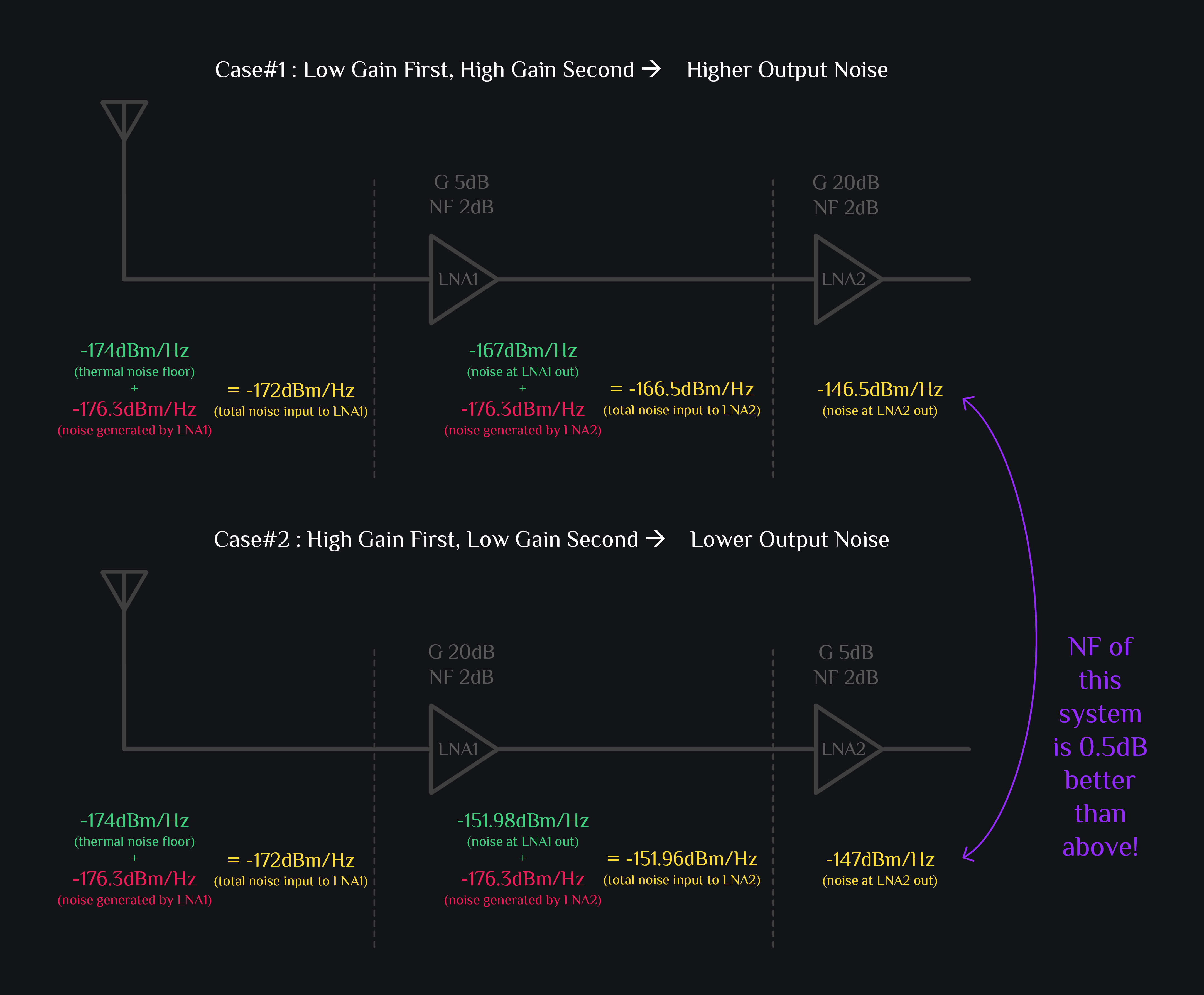
But what are you telling us? We ourselves are amplifying noise to suppress noise of subsequent blocks? Sounds ridiculous. We would still end up with so much noise. The answer is you were going to get this much noise anyway. If your RX has 25dB gain, it was going to amplify noise by 25dB anyway, only question was how do you distribute this 25dB gain between blocks. If you use high gain block first and low gain block second, you save yourself from the additional noise added by the second block. Ok, so how about additional noise of first block. How can we suppress that? There is no suppressing here. And that is why the concept of low noise amplifier (LNA) exists: LNA or the first block in your RX should have as high gain as possible and as low noise as possible. If you want to nit pick, yes noise of first block can be suppressed provided that your input noise was high anyway (e.g., we assume -174dBm/Hz input noise, but what if antenna is picking up some background noise and your input noise is -140dBm/Hz to begin with? then NF of your first block also wouldn’t matter/add much)
Download noise figure calculator.
So the talk in the town is that you can predict your IM3 from a single tone test: that is excite your system with single tone and measure HD3. IM3 is three times higher. Just measure HD2 and IM2 is two times higher.
Then why don’t you see it in measurements? Because assumption here is that your system is weakly non-linear which means you can model your system by third order polynomial, you don’t need higher order coefficients. This assumption is not true in actual practice. You do see fifth order non-linearities e.g., finite HD5 or finite IM5. In that case, classical IM3 and HD3 relations don’t hold. By same token, formula that states IIP3 is 9.6dB higher than P1 dB does not hold. Why the heck do we keep teaching it then? Let us know if you know. See intermod analysis for more details.
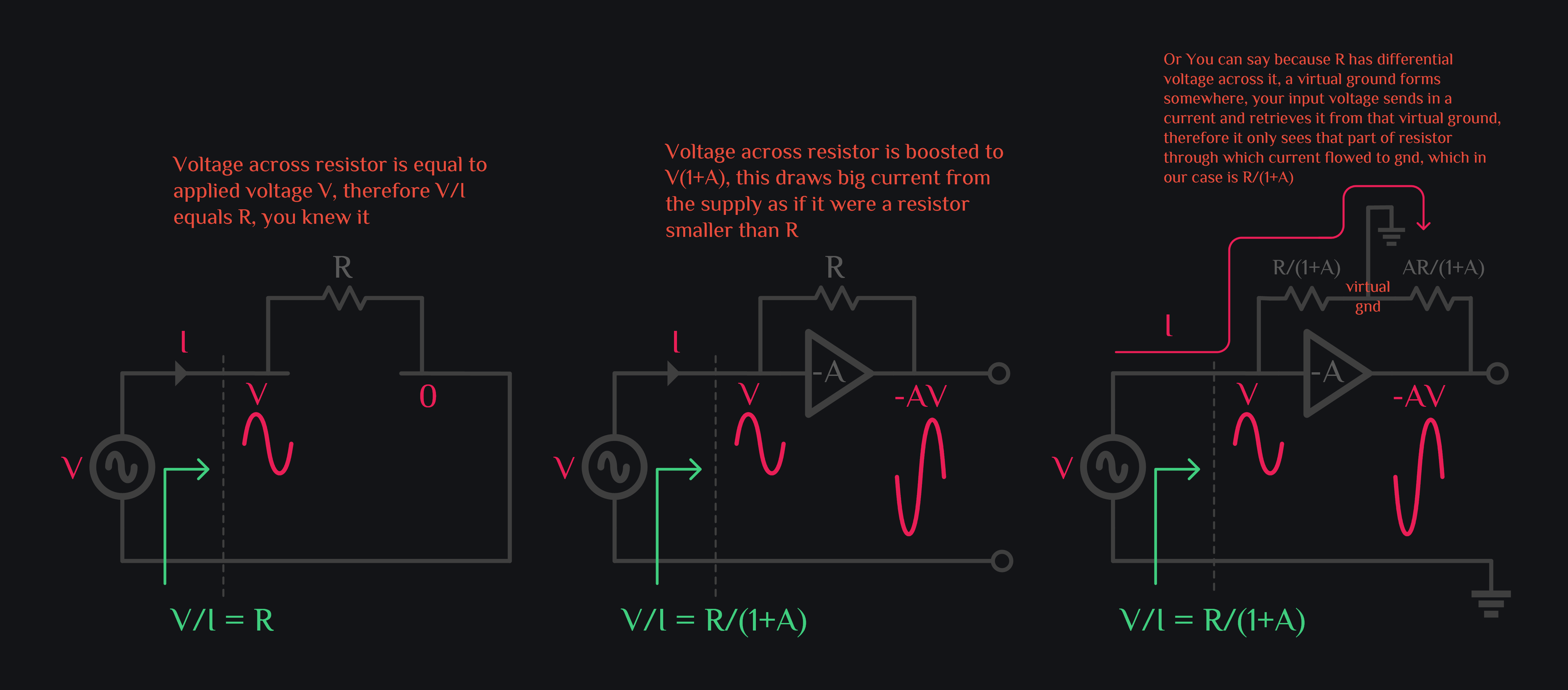
Consider a resistor R connected across an inverting amplifier with gain -A. Input impedance seen by source is reduced to R/(1+A) as expalined in image below.
Miller effect also says the same: your CGD capacitor connects between drain and gate of transistor. And transistor is an inverting amplifier. Therefore input impedance is reduced by 1+VoltageGain of circuit. Reduced input impedance means capacitance would have increased.
\(f_\tau\) is the frequency where current gain of a device drops to one whereas \(f_{max}\) is frequency where power gain drops to one. \(f_\tau\) is mainly a metric for device designers where they seek to minimize carrier transport time across the device. \(f_{max}\) is a metric for circuit designers where they seek to maximize operating frequency of transistor embedded in a real circuit will all parasitics and load source impedances accounted for. Checkout details here.