mm-Wave PA Design Tutorial
Power Amplifiers (PA) are in the transmitting chain of a wireless system. They are the final amplification stage before the signal is transmitted, and therefore must produce enough output power to overcome channel losses between the transmitter and the receiver. In this tutorial, we are going to have a detailed look at mm-wave PA design.
mm-Wave PA Design Metrics
Before we head out to design PA, let’s see some important design metrics we design around:- Peak Output Power
- We desire high output power as it determines two-way communication range
- Efficiency
- Longer battery life (e.g., wireless handset)
- Lower operational cost (e.g., cellular basestation)
- Usually the 2nd most important specification after output power
- Power Gain
- Typically, we desire high gain as it relaxes design of preceding stage
- Power added efficiency reaches collector efficiency for high gain systems
- Stability over VSWR
- Ability to transmit into unknown/varying load “Unconditional Stability”
- Linearity
- Faithfully transmit input signal to output
- Control spectrum leakage to minimize interference to other user
Design Goals for this Tutorial
- Design goals:
- Frequency: 94 GHz
- Output Power (P1dB) : 10dBm
- Power-added Efficiency (PAE): As high as possible
- Transistor:
- 0.13um BiCMOS SiGe
- Peak fmax: 500 GHz
- BVCEO : 1.7V
- BVCBO : 4.8V
- Softwares:
- Keysight ADS : Circuit simulations
- SONNET: EM simulations
- Cadence Virtuoso: Layout
Step #1: Topology Selection
The first step in designing a PA is topology selection. Let’s look at the standard amplifying blocks shown in image below. We have common emitter (CE). It has high input impedance and high output impedance which is great. Reverse isolation is poor because there is miller capacitance between collector and base. And also the output power is limited by the collector emitter breakdown voltage, BVCEO.
The next candidate then is common base amplifier (CB). Common base voltage swing would appear across collector and base. CB can produce higher output power as it we can put higher voltage swings voltage across it compared to CE (BVCBO > BVCEO). But, the input impedance is very low, making it very difficult to drive.
Next we have cascode, which has properties of both common base and common emitter. Upper transistor works as common base, generating higher output power. Lower transistor is common emitter, providing higher input impedance. Also there is no direct feedback capacitor from output to input, thus reverse isolation is also very good. It makes sense to go for cascode, so go the most of mm-wave PA designs.
Step #2: LoadPull Simulations
PAs are designed using loadpull simulations because:
- BJT models (hybrid-pi, T etc.) are based on small signal approximation
- PA output comprises of large signals (voltage, current or both)
- Large signal impedances are different than small signal impedances
- LoadPull analysis determines optimum large signal load impedance for the highest PAE and Pout
Here’s how to launch Loadpull workbench in Keysight ADS software, as shown in image below.

We have chosen cascode as our core amplifier and connected it to the load pull instrument as shown in image below. Our goal was 10dbm. Let’s do 13dBm in order to accommodate losses (3dB higher? let it be, this is 94GHz you are talking about).
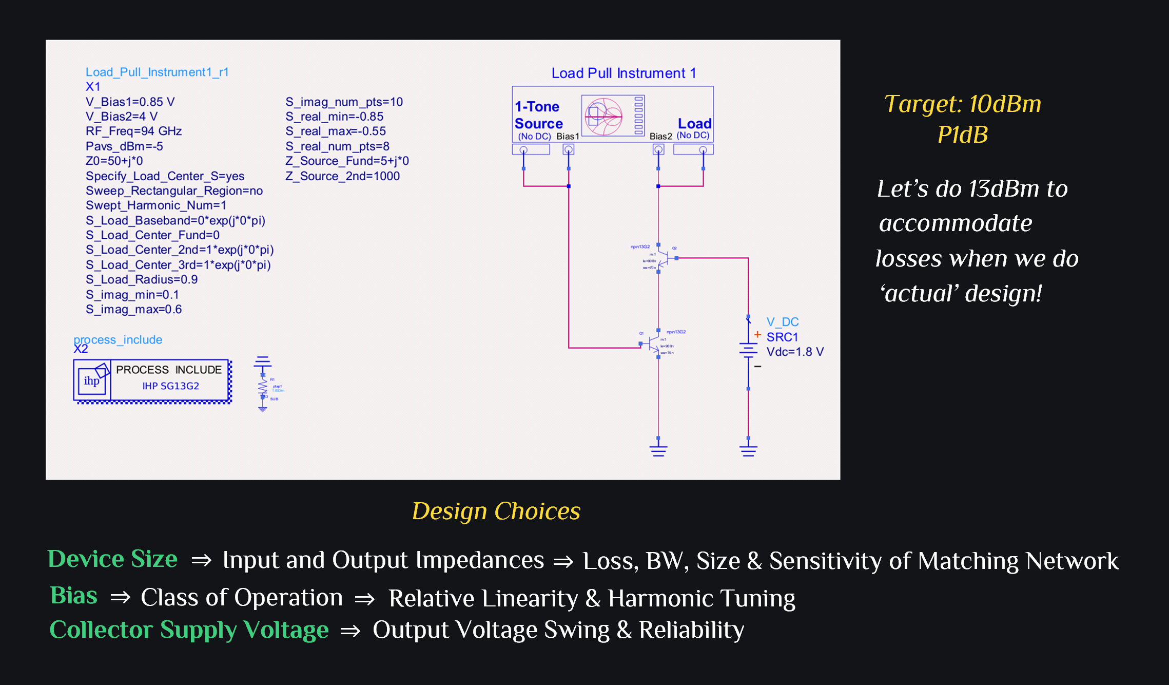
We are going to run multiple load pull simulations to optimize device size, bias, and supply voltage:
- Device size: If we increase device size, we increase the output power. However, input output impedance may become too low which makes the design of matching network very complicated. It gets lossy, narrowband, and sensitive to component values. So, generally we trade off between matching capability and output power. For example, if the impedance we are matching to is around 1-2\(\Omega\), we would stop there and not increase the device size anymore.
- Bias Voltage: This will determine class of operation and tunability capability. If you bias in class B, you can utilize harmonic tuning or waveform engineering to enhance efficiency (ah? check this). We are starting simple, so let’s move on with class AB biasing.
- Collector Supply Voltage: This directly relates to output voltage swing. Of course, the higher the supply the better, but then we do not want to exceed breakdown limit as well. So, we have to choose it carefully based on breakdown limits.
a) Run LoadPull
Run loadpull simulation. Start with approximate bias settings, input power, device size etc. and tune them as you optimize loadpull impedance. We start with 0.8V VBE of input transistor, 1.8V at cascode base and 4V VCC. Please read plots below from left to right. These are loadpull iterations we did. We highlight in yellow color what we changed in each simulation.
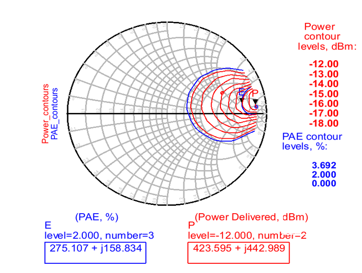
- Transistor size: 1×0.9umx0.07um
- Pavs : -5dBm
- VB_lower = 0.8V
- VB_upper = 1.8V
- VCC = 4V
Comments: Not even amplifying. Need to increase VBE.
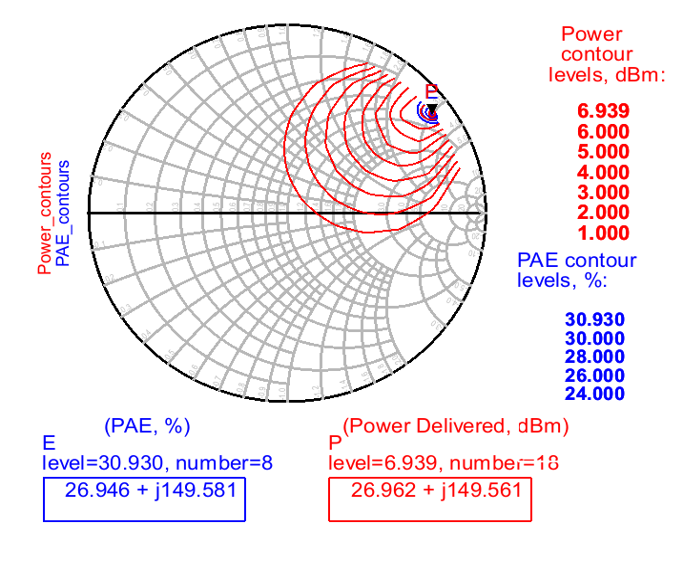
- Transistor size: 5x0.9umx0.07um
- Pavs : -5dBm
- VB_lower = 0.85V
- VB_upper = 1.8V
- VCC = 4V
Comments: Amplifying. Source impedance is not optimal right now. It can produce more power probably. Inrease Pavs.
- Transistor size: 1×0.9umx0.07um
- Pavs : +5dBm
- VB_lower = 0.85V
- VB_upper = 1.8V
- VCC = 4V
Comments: Getting closer to target value.
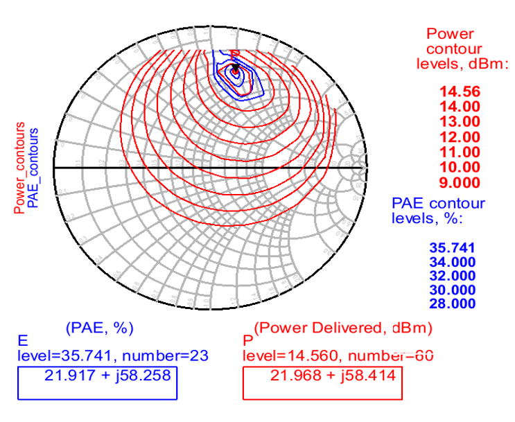
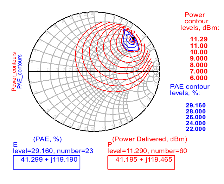
- Transistor size: 10x0.9umx0.07um
- Pavs : 5dBm
- VB_lower = 0.85V
- VB_upper = 1.8V
- VCC = 4V
Comments: 13dBm achieved. But is this the max PAE that we can achieve? Maybe not. Bias point may not be optimum, source impedance is not correctly set. Let’s do source pull first.
b) Run SourcePull
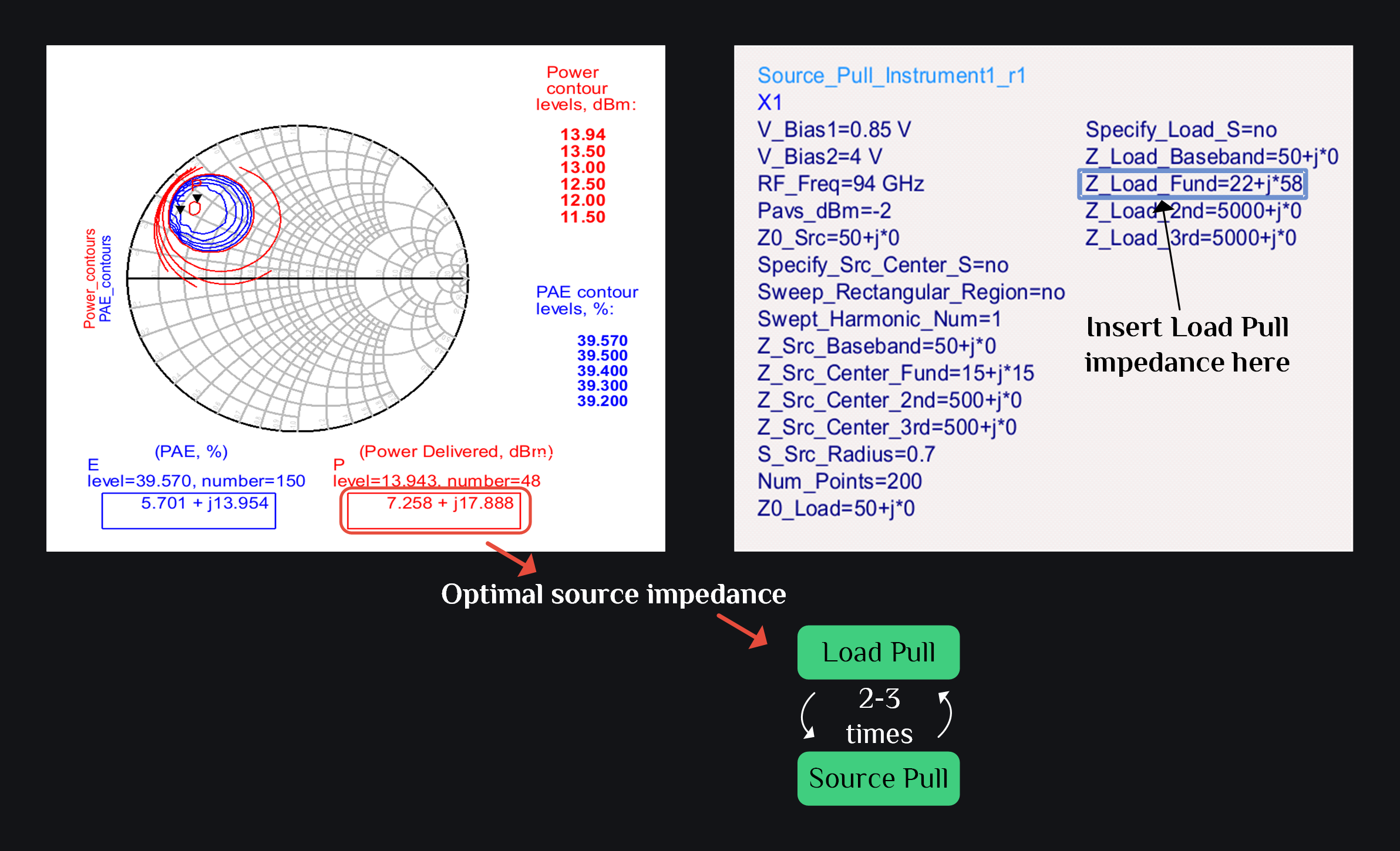
Insert the loadpull impedance (center point of converged contours shown in bottom right image above) in sourcepull setup and run sim.
- Transistor size: 10×0.9umx0.07um
- Pavs : -5dBm
- VB_lower = 0.85V
- VB_upper = 1.8V
- VCC = 4V
Comment: We don’t need to overdrive the PA, so Pavs has been decreased.
c) Run LoadPull Again
Run loadpull. Use loadpull impedance and Run sourcepull. Use sourcepull impedance and run loadpull. Repeat this a couple times until you have converged to a loadpull and a sourcepull impedance.
We got following:
- 13dBm P1dB (we swept power to confirm if it is indeed P1dB)
- 41% PAE
- \(19+j\,63\,\Omega\) LoadPull Impedance
- \(7+j\,18\,\Omega\) SourcePull Impedance
- Pavs : -5dBm
Comment: We don’t need to overdrive the PA, so Pavs has been decreased. Alright, we are done with loadpull of mm-wave pa.

Why max PAE is limited to 41%?
We biased in class AB which would typically have efficiencies around 50-60%. This is true for low frequencies where parasitics can be ignored and design follows the simple math. But at 94GHz even the fF of capacitors matter! And they make voltage and current waveforms overlapping, so there is power dissipation across the device which degrades the efficiency.
Step #3: Large Signal HB Simulations
a) Sanity Check
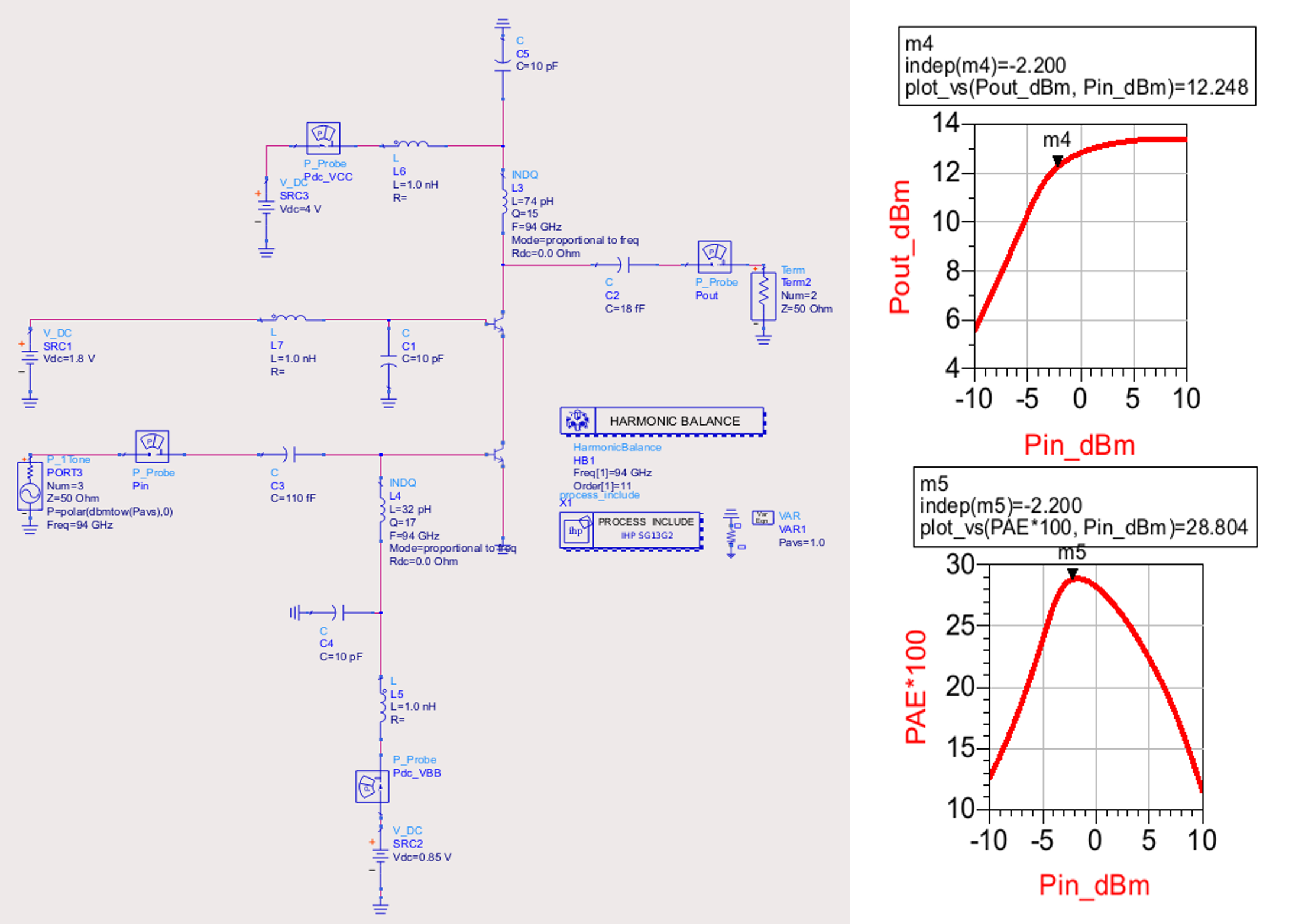
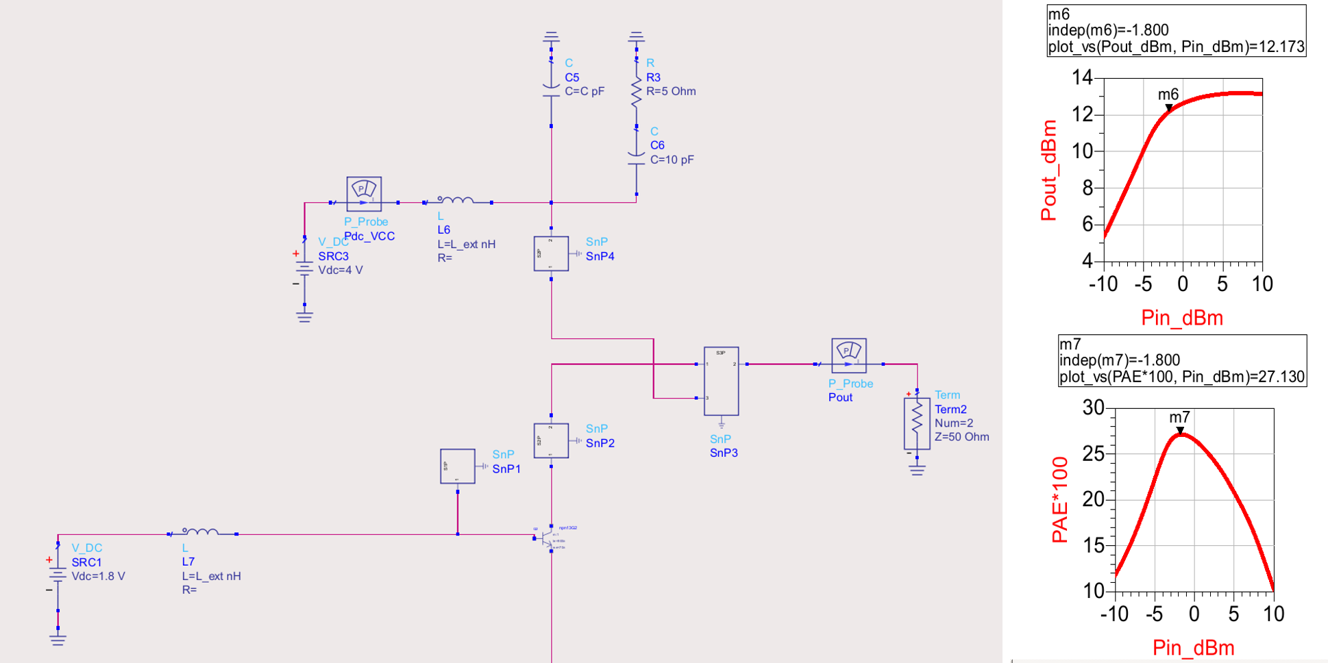
Terminate the PA with load and source impedances found above and do harmonic balance analysis with power sweep. Setup is shown in image below.
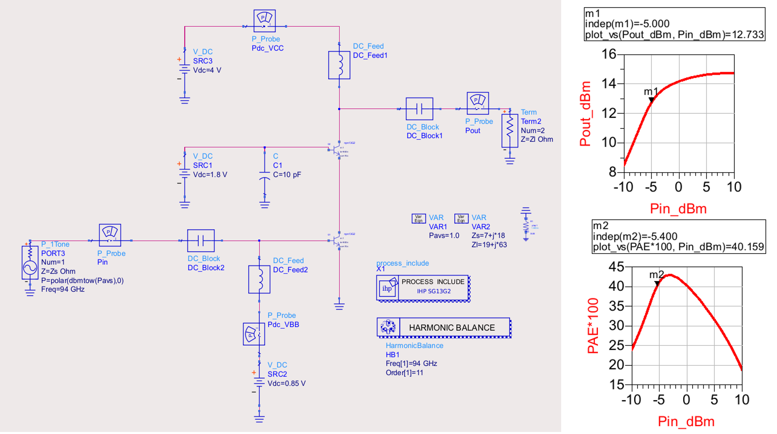
Results are very close to loadpull simulations but not exactly the same. Why? Because harmonic impedances are not open-circuited in this case. We observe our peak PAE
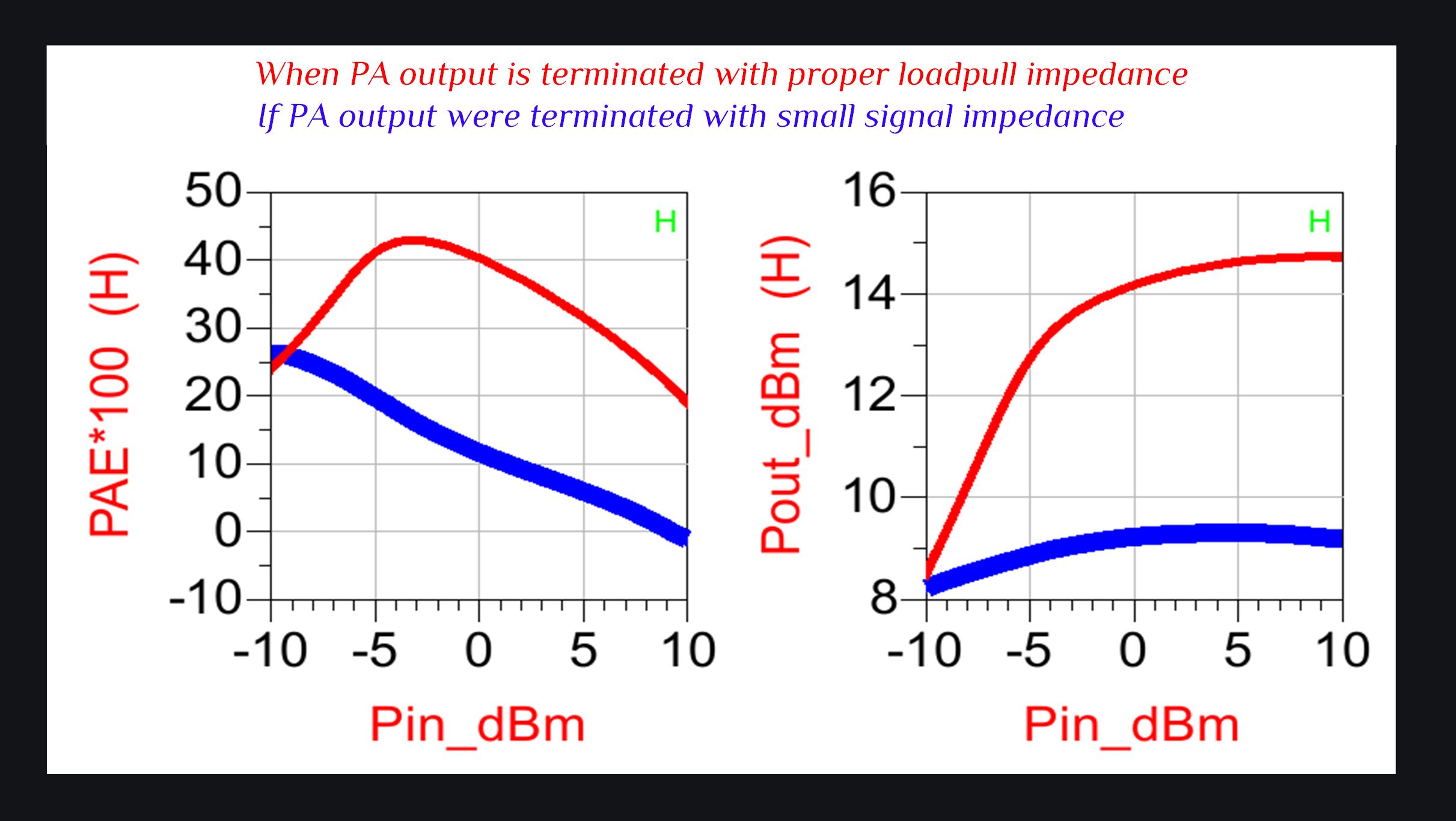
b) Comparison of small and large signal impedance
Before we proceed, let’s just see for the sake of our understanding, the difference between small and large signal impedance. Run an s-param simulation and compare how does it look against source and loadpull impedances. We found that sourcepull impedance was very close to S11 but loadpull was very different than S22. It makes sense because the output experiences large voltage swings, and hence its large signal impedance is different than small signal s-param impedance.
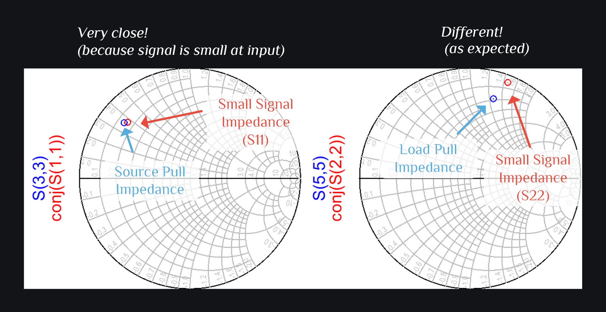
You clearly see in image below that if you were to proceed with small signal matching of your PA, your Pout and PAE would have been crap.
c) Design Matching Network using ADS Smith Chart Tool
Four possibilities using L-match. Choose the one which suits your needs.
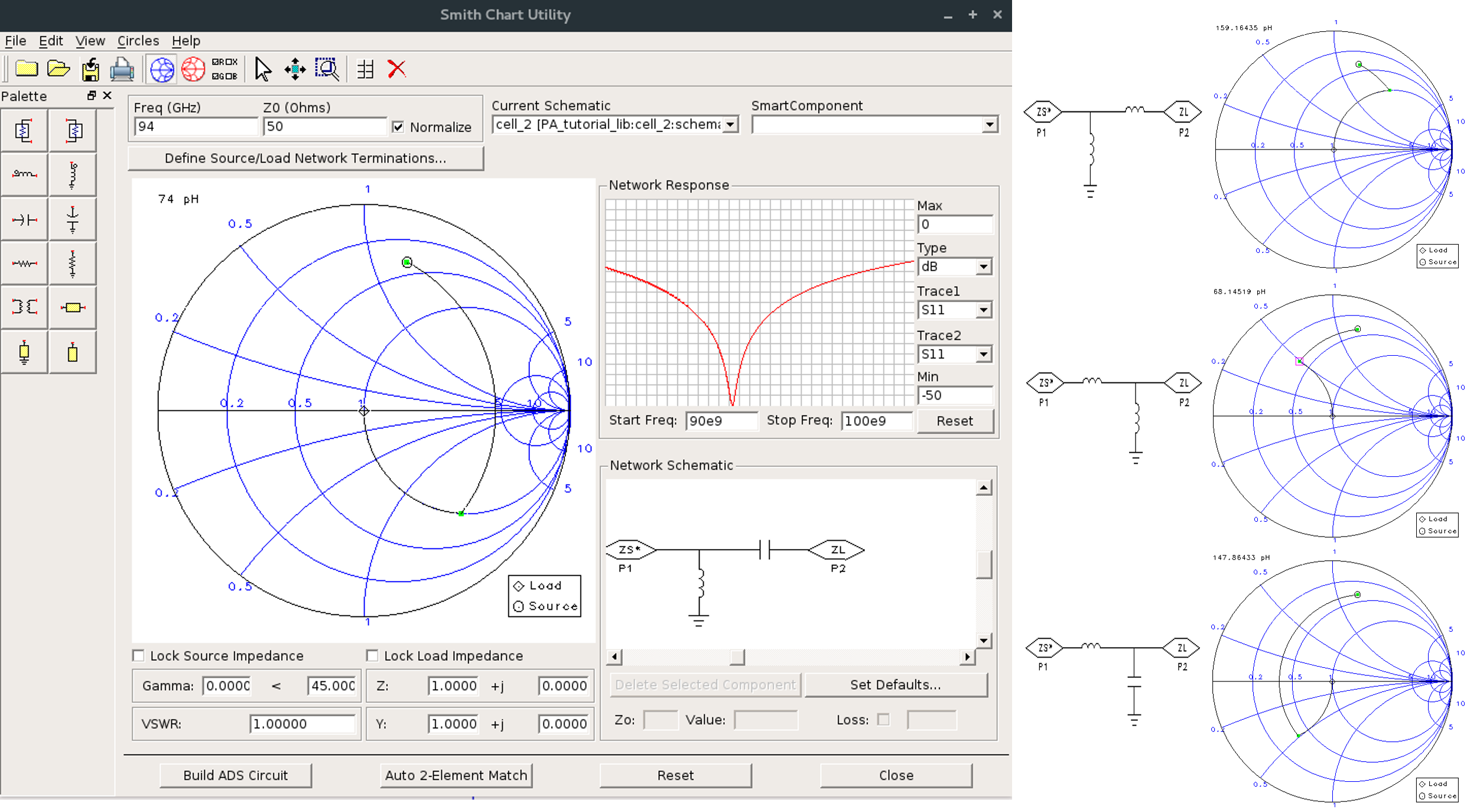
We have chosen the first one with shunt inductor and series capacitor. We will bias out collector through shunt inductor and use this capacitor as DC block for output. Hence, this network serves as a matching network as well as bias T for mm-wave pa.
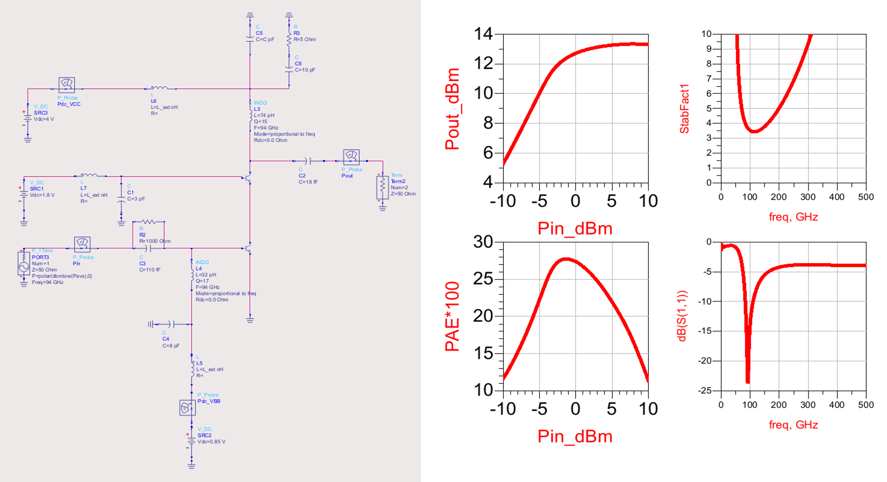
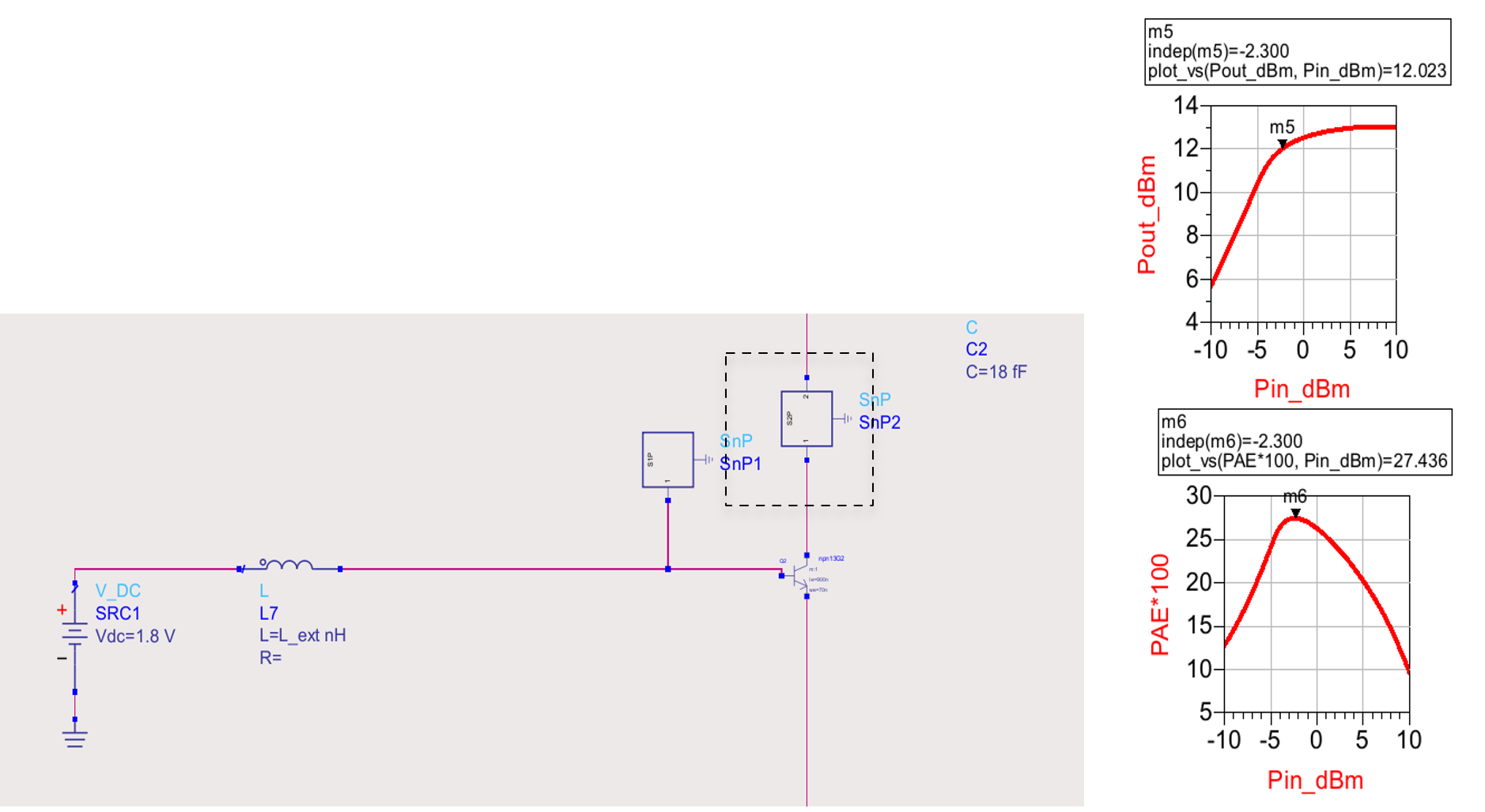
d) Run HB with Matching Network – Ideal Components
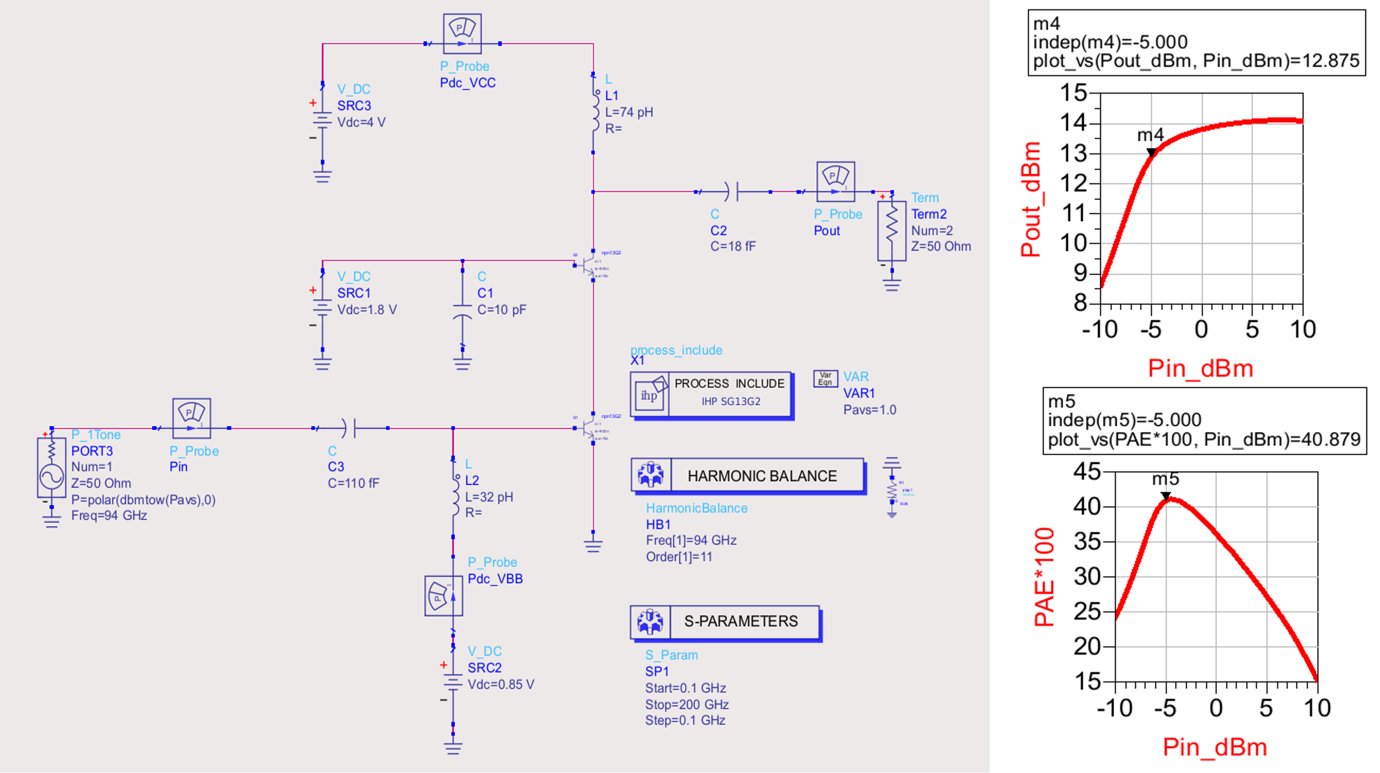
We are on track. Pout and PAE after matching match loadpull simulations.
e) Run HB with Matching Network – Components with Q
It is good practice to use approximate Q of components and run sims. Things will degrade but we want to know how much before we go into EM sims. Also a good idea to run loadpull again with these losses. If loadpull impedance is same as before, you should see loadpull contours converging to \(50\,\Omega\). If that is not the case, it means losses have changed optimum loadpull impedance or your open-circuited harmonics are no longer open as seen by PA looking thru matching network to \(50\,\Omega\). Tune the matching network values till you make it to \(50\,\Omega\).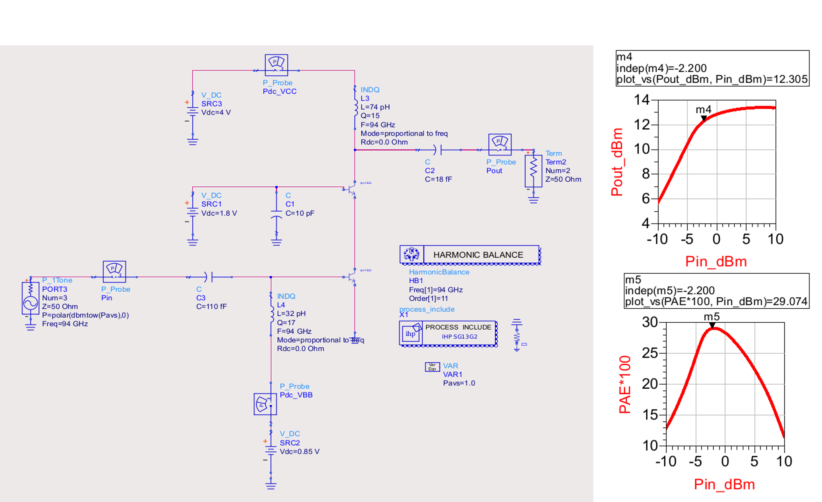
We added Q to inductors. Two things happened. First because of the loss at output inductor, our Psat has decreased by 0.5dBm and our PAE has decreased by 12%. Second, the gain saw a big reduction because it takes into account both input and output losses. Now, our peak PAE is not at -5dBm but -2dBm.
f) Replace Ideal Voltage Sources
Replace ideal voltage sources with realistic models:
- DC probe or Wirebonds will have inductance
- Put on-chip decouping/bypass caps
Adding wirebond inductances and bypass caps didn’t impact Pout or PAE. Phew. Let’s move on.
Step #4: Stability Tests
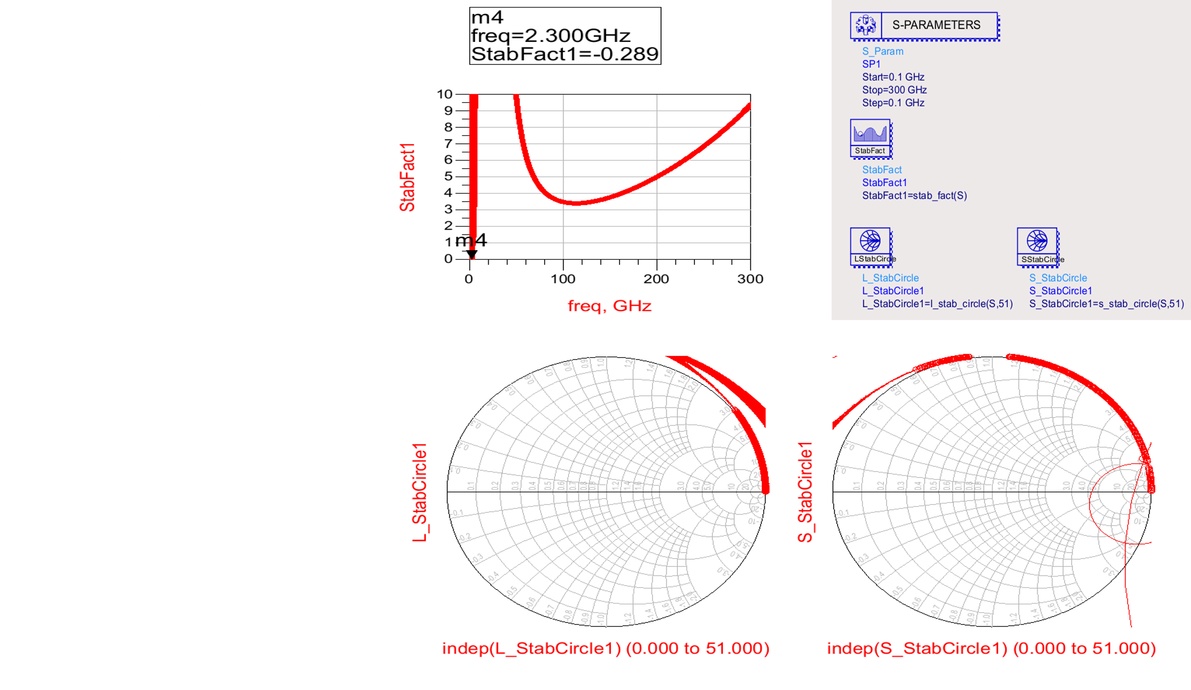
a) Simulate k-factor
Use s-param simulations and StabFact in ADS. Note that there is ever going debate on what is the correct test for stability as some folks do not like small-signal stability tests on devices which operate in large signal. You should do your due diligence to run different tests for stability after you are done with design (like run a transient sim, no one would argue on that). However, to progress through design optimization stages, we think k-factor or mu are good enough. So, let’s run k-factor (StabFact in ADS) and see what happens.
b) Add series resistor at base
Add a series resistor at base to stabilize source and make sure bypass cap is sufficient for low frequencies.
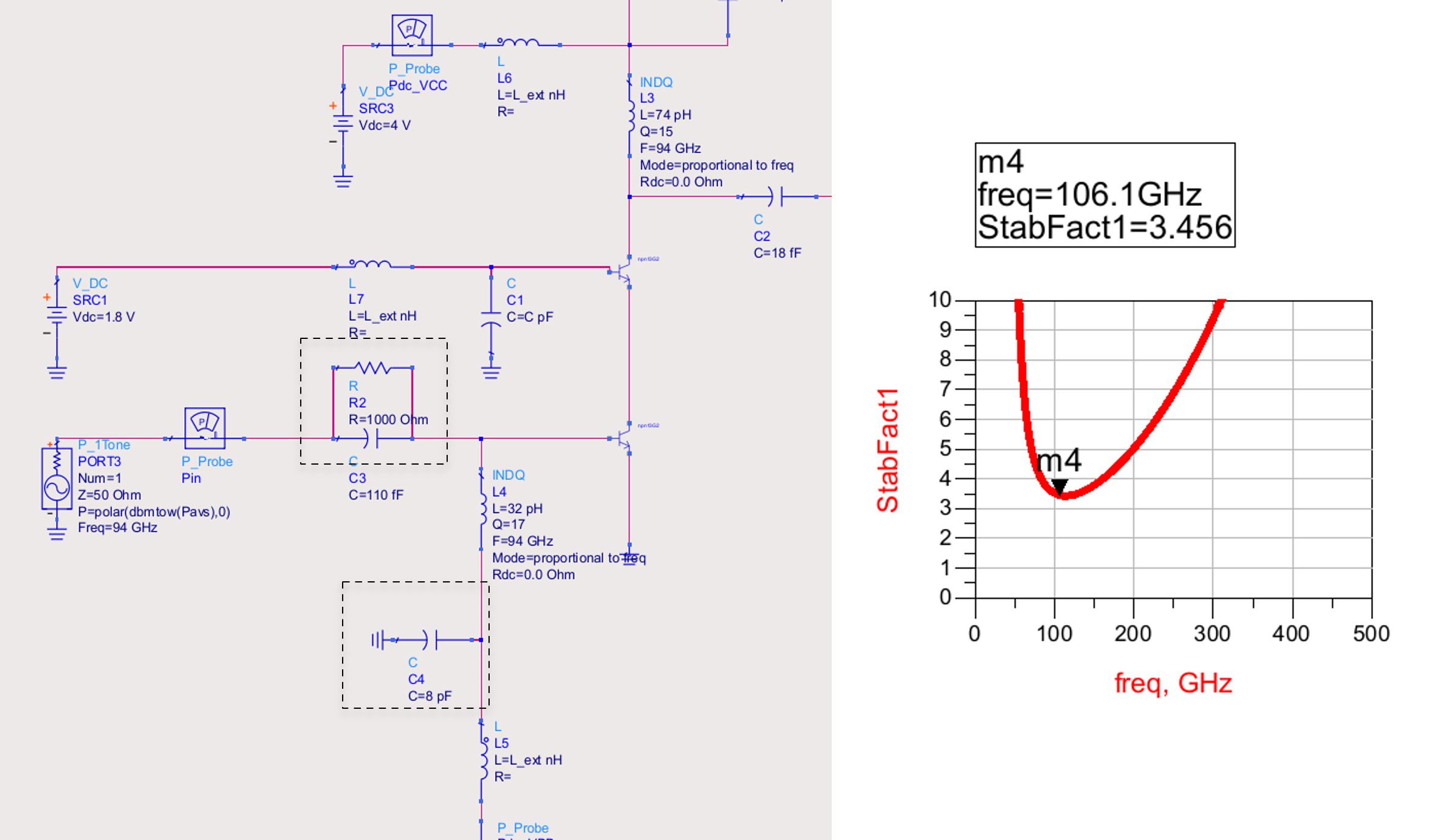
c) De-Q VCC node
Although PA is stable now, add a de-qued capacitor at VCC node just as a precaution (because we know this node has tendency to get unstable)
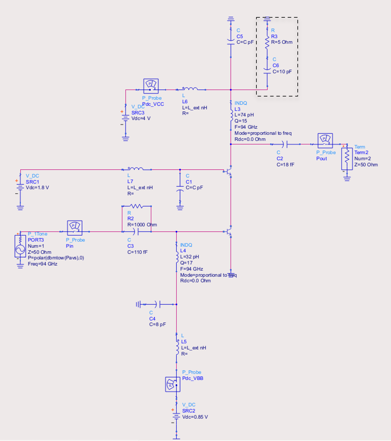
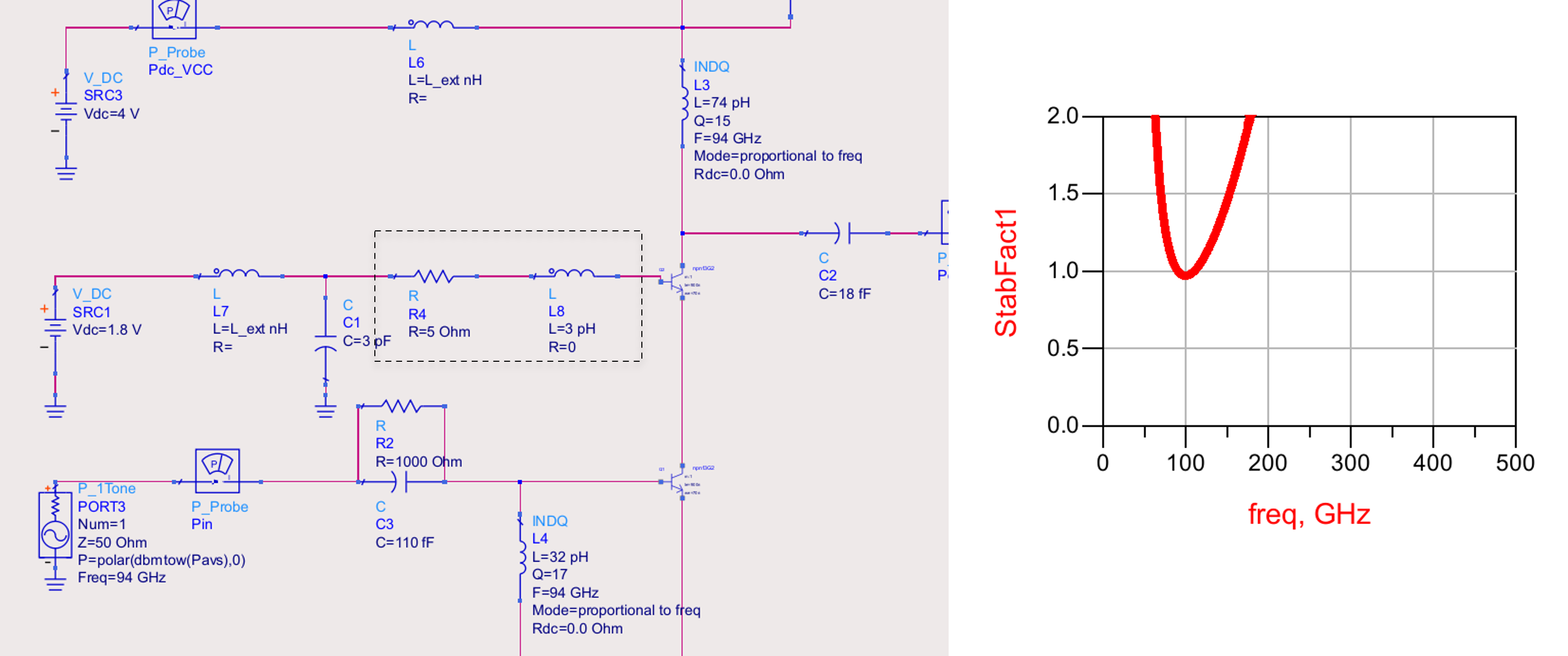
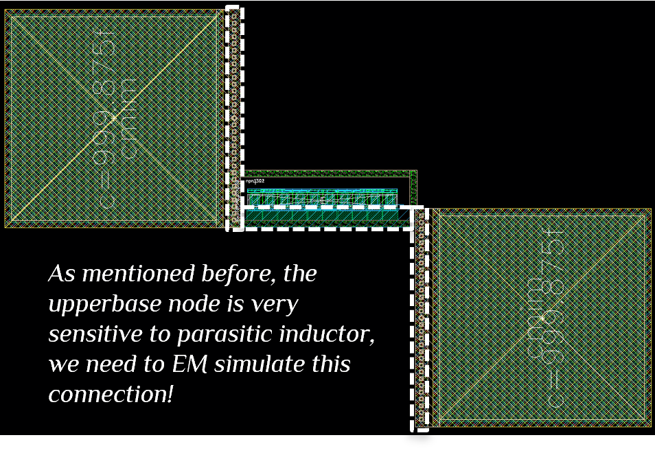
d) mm-Wave PA special: Upperbase node
Upper base node is highly prone to oscillation in mm-wave power amplifiers. Even a little parasitic inductor (~5pH) can make PA oscillate. Add a parasitic inductor, and see what happens:
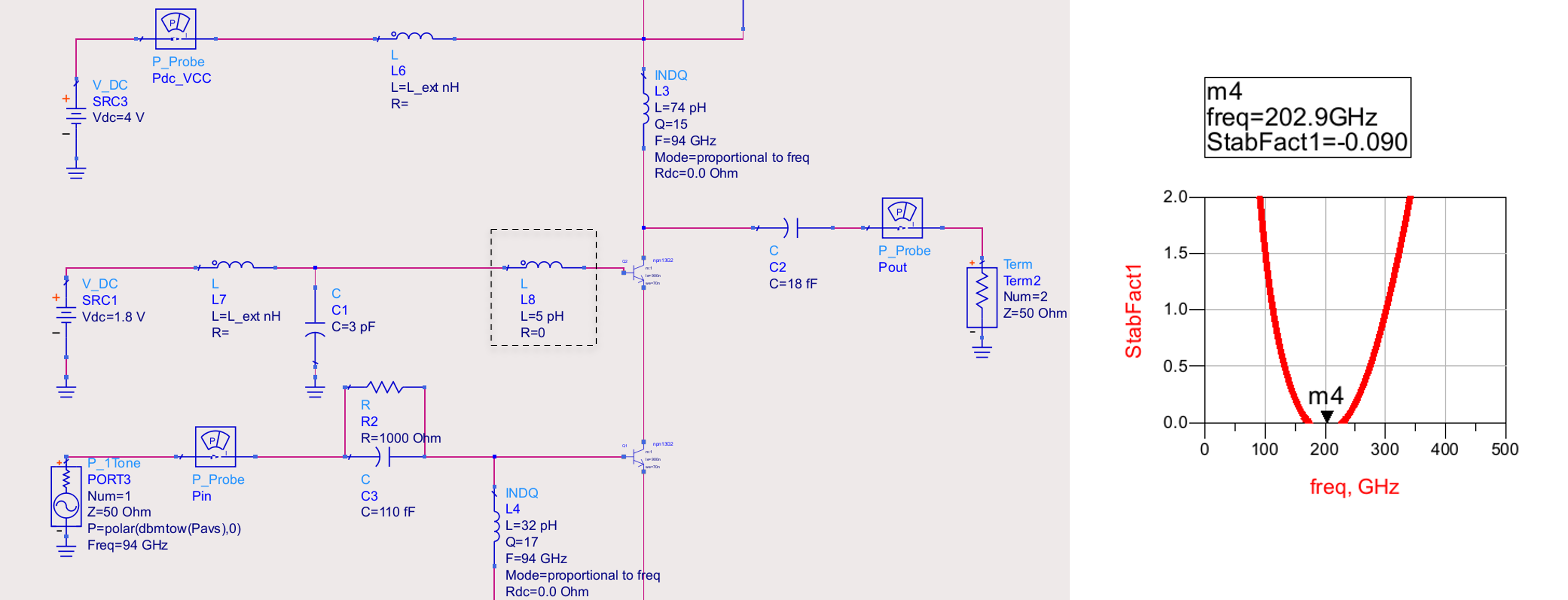
The only way forward here is to reduce parasitic inductance as much as possible or introduce loss. We show that adding \(5\,\Omega\) resistance solves the issue (StabFact > 1)
Step #5: Catch a Break. Schematic Level Design Completed.
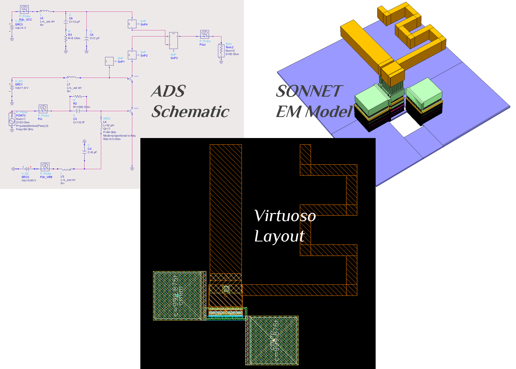
Step #6: EM Simulations
a) Get to know your process
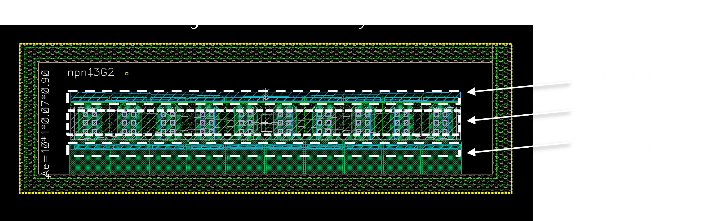
We are going to use a process which has 5 thin metal layers (M1-M5) for general purpose routings, 2 thick top layers (TM1-TM2) used for RF routing, MIM capacitors and Rsil Rppd resistors. This is how a transistor looks in our PDK:
b) Layout the Most Sensitive Routing
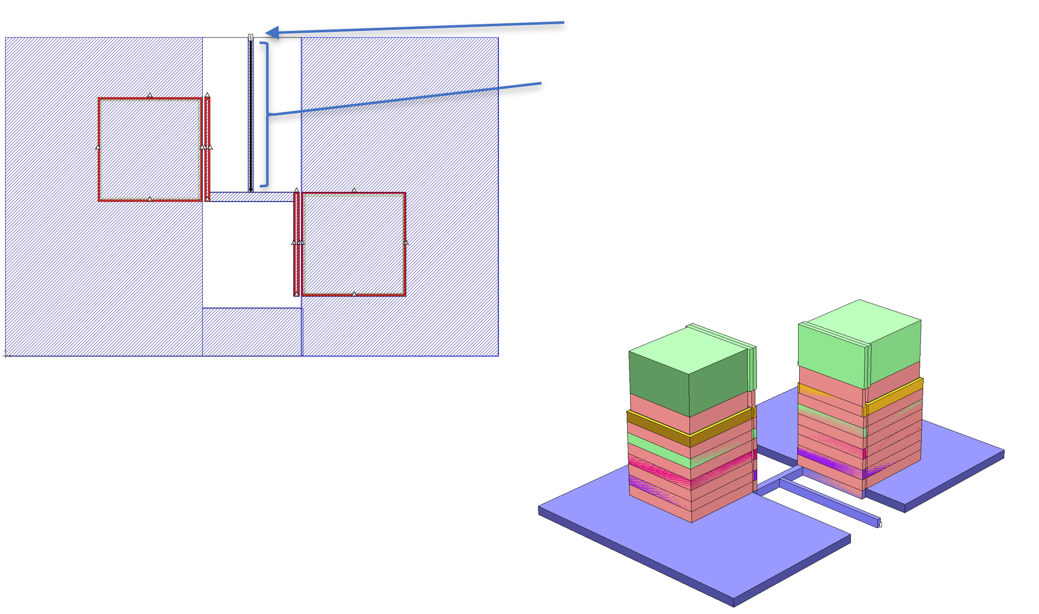
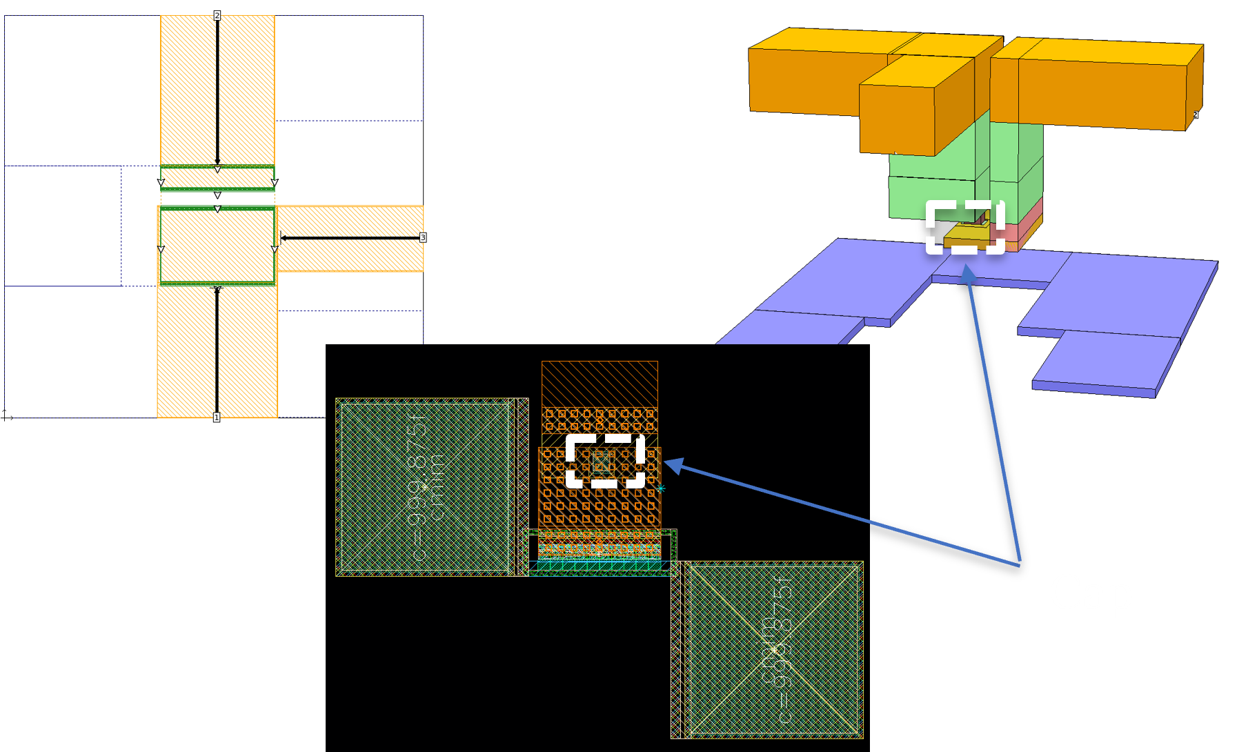
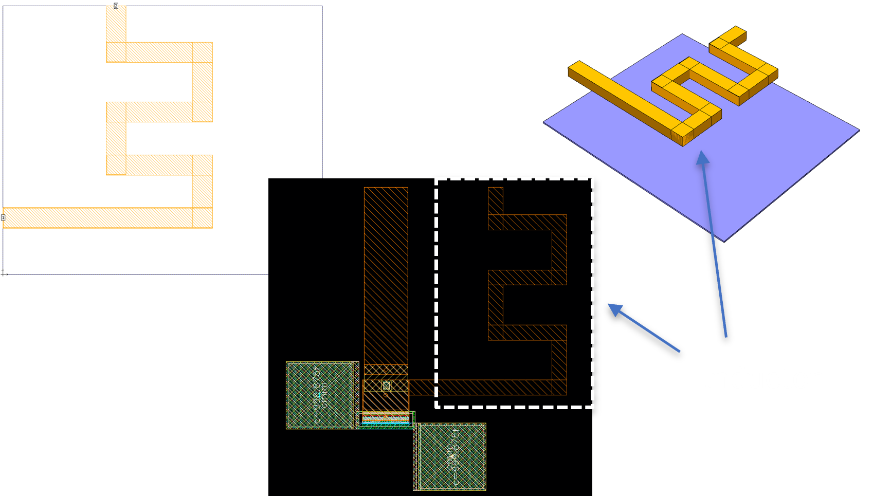
Make a floor plan of where do you want things to be. We start with upperbase connection before anything else since we know this node needs the lowest inductance possible for stability of mm-wave cascode.
c) EM Modelling in SONNET Software
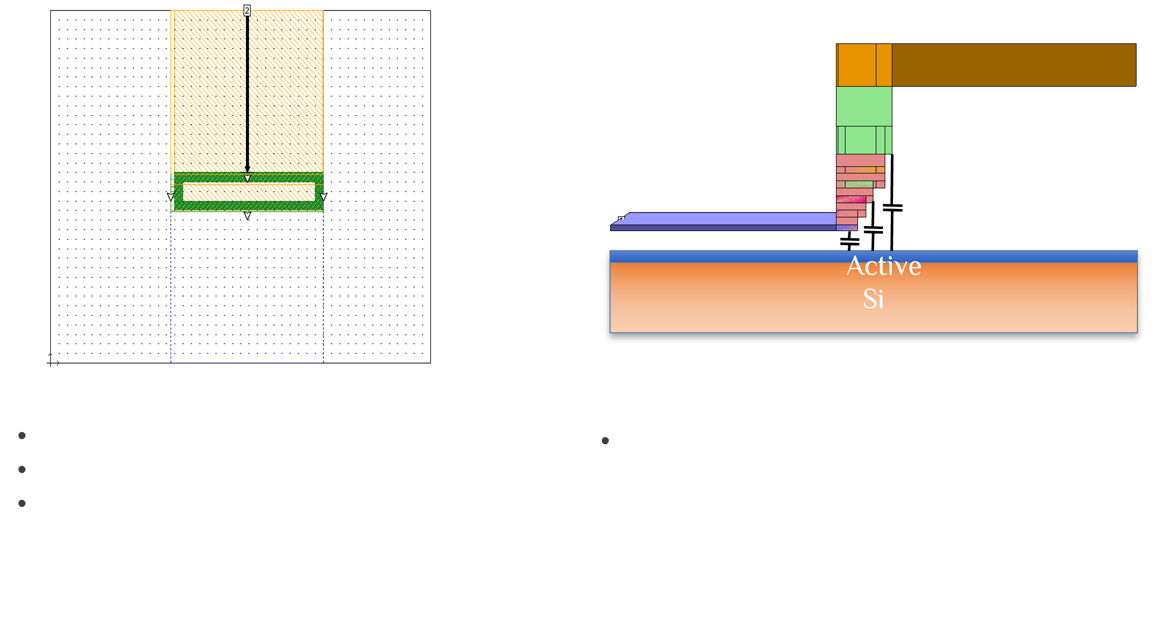
You can use whatever EM software you have available. We had Sonnet. In the image below, we show routing from the base node of cascode to the top metal layer. In Sonnet, your structure is enclosed in a closed metal box which serves as a ground reference. “BoxWall” is a port which connects between this metal box and your feedline and then you de-embed your feedline (it’s similar to Waveport in HFSS software). Read more on Sonnet in [1] & [2] if you are interested.
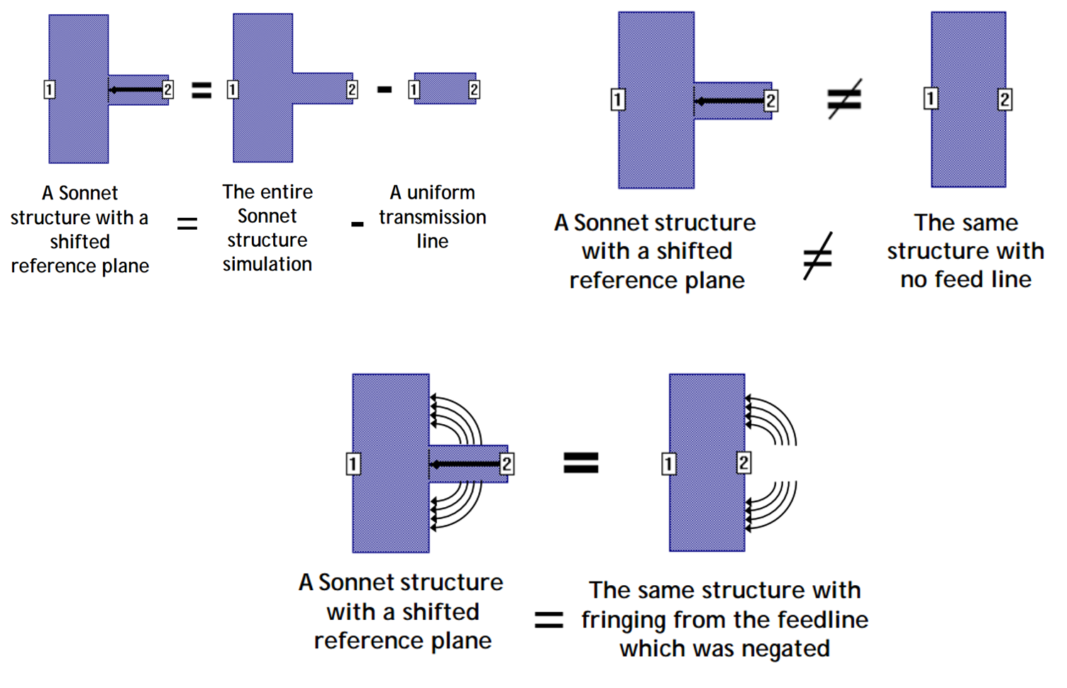
Worth mentioning that a common misconception about de-embedding: it completely de-embeds feed line. Not correct. Fringing fields are not de-embedded as shown in image below [2].
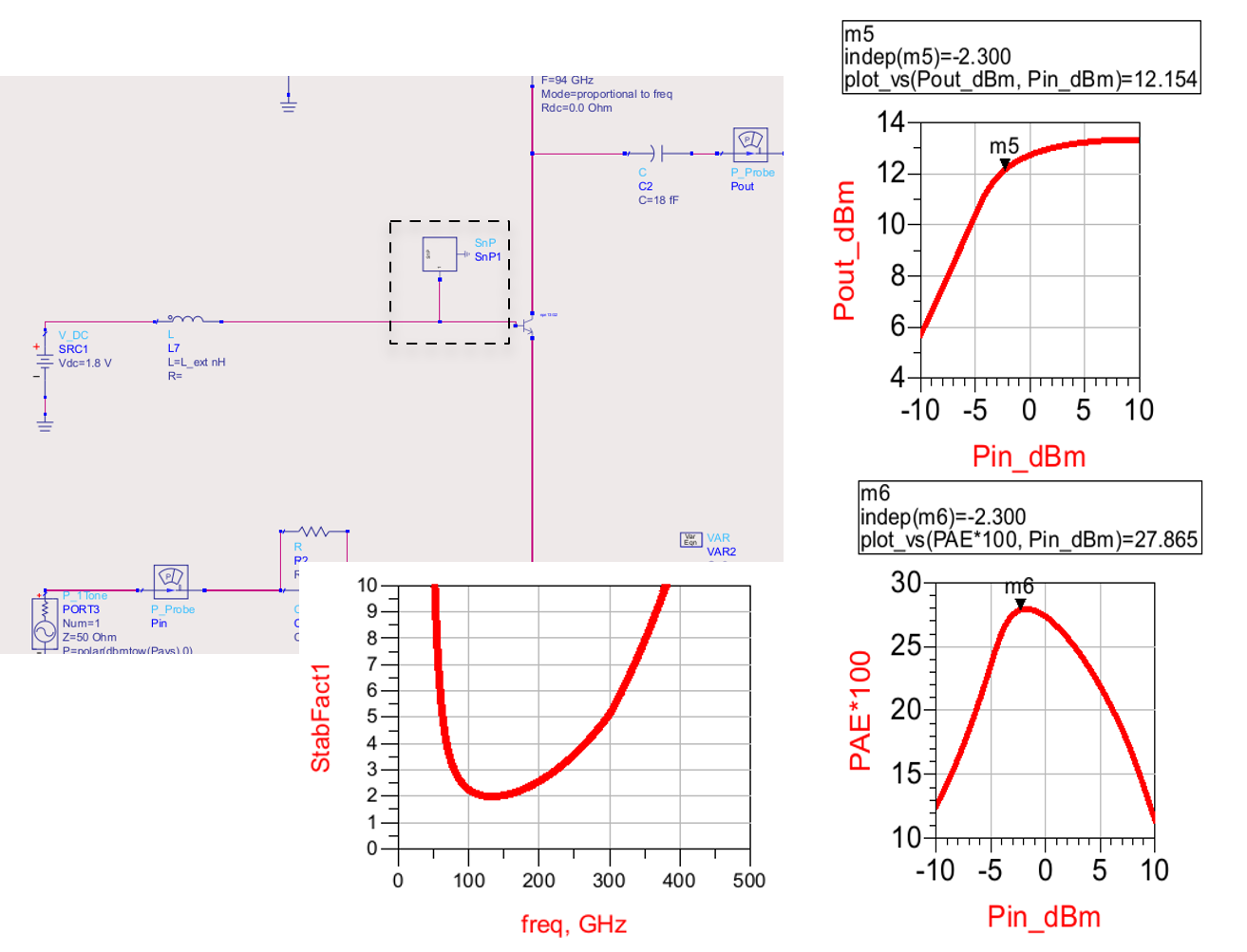
Export s-param model from EM sim. Attach it to your schematic, and run HB and s-param sim. We see that k-factor is greater than 1 showing that it is unconditionally stable. We did a good job in minimizing the inductance of this connection.
d) EM Sim of Output Matching Network
Connection from transistor collector on M1 to layer to topmost layer (TM2).
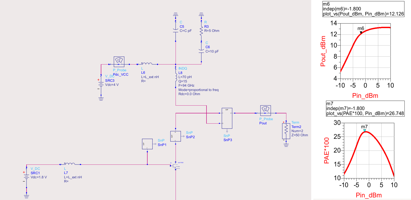
Insert exported s-param in schematic and run sim. Results look great. Very little drop in Pout and PAE.
Add matching network capacitor in EM sim
Insert exported s-param model in schematic and simulate.
We are doing this step by step to keep track of where do we lose performance. Losing 1% PAE or 0.2 dB of power is not a big deal, it maybe because matching is not EM optimized yet. Keep on adding more stuff and optimize it later altogether (optimize in small groups if things get out of control).
We added output matching inductor. Let’s run the sim.
Results look great. At this point, simulate all the EMs together (base connection, output cap and ind). Optimize and re-simulate. Few iterations and you should be close (however, we should mention this process of optimization is very tiring and you don’t actually do “few”, you do a lot EM sim, optimize, EM sim, optimize…it’s frustrating. Don’t worry, AI is coming to help, and beside in Industry you don’t need to do this, they have hired folks to do these optimization for you)
e) EM Optimized Matching
Here is how our optimized layout for upperbase connection and output matching looked like. We did not do input matching. Give us a break. We think you got a pretty good idea what’s the process like. This completes our design of mm-wave PA.
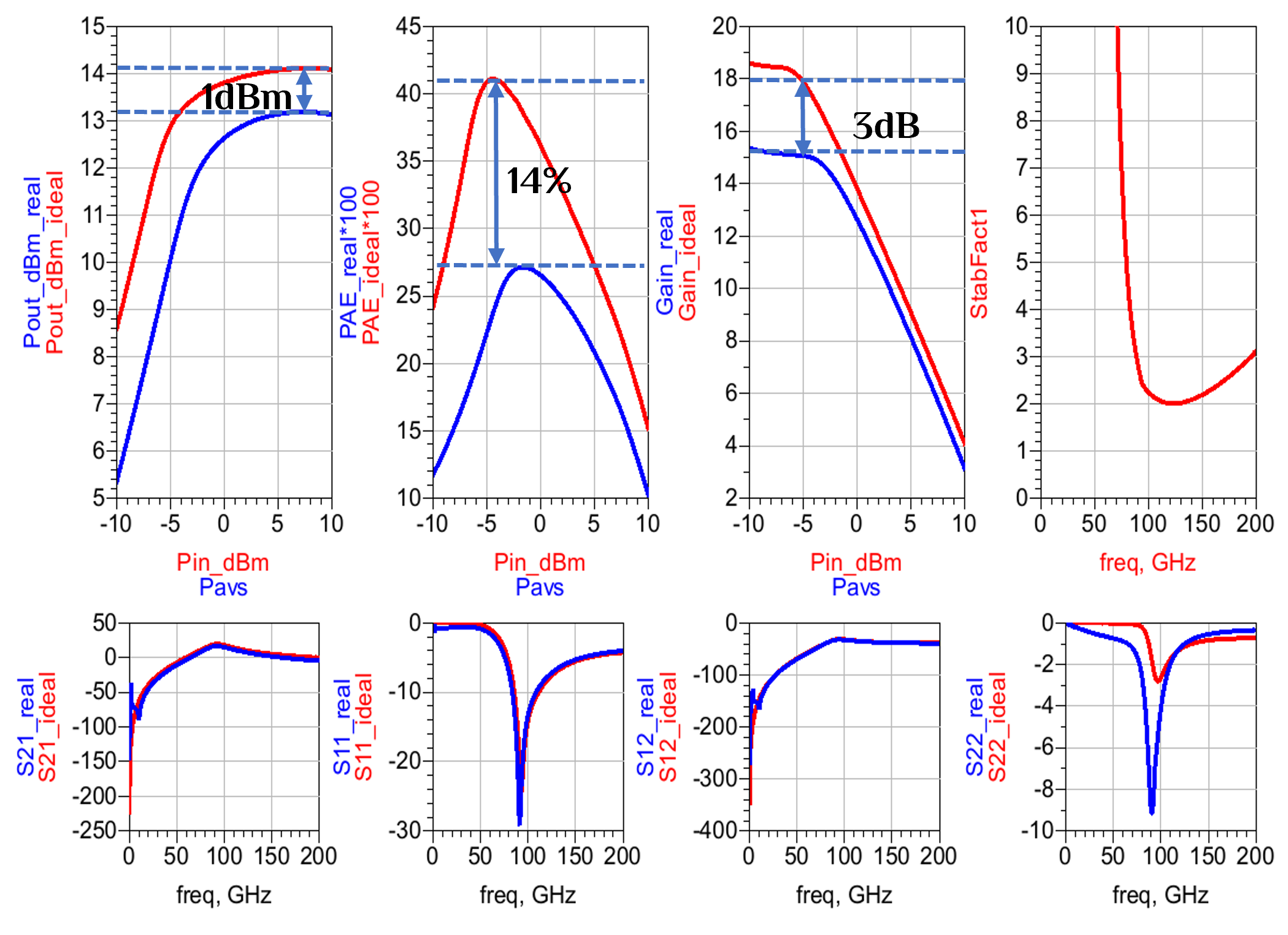
These are the final results. Just for fun, we compare with ideal components vs layout. We see 1dB loss in Pout, 14% drop in PAE and about 3dB drop in gain. Also interesting to note that s-param look quite the same. At this point, you have one design ready and you know what to expect from a 94GHz PA. Now is the time for you to get creative and start thinking of matching networks other than L-section to reduce the loss. There is an optimum for matching network order that give you the lowest insertion loss. Yes, lower number of elements are not always lowest in loss. Intuitively adding sections can decrease the insertion loss since it also lowers the network Q factor. Adding too many sections, though, can counterbalance this benefit. Check last two slides of Niknejad.
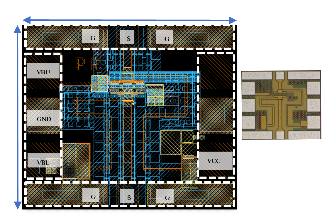
Actual Tapeout
We taped out a PA designed at 28GHz using above steps. Image below shows chip photo.
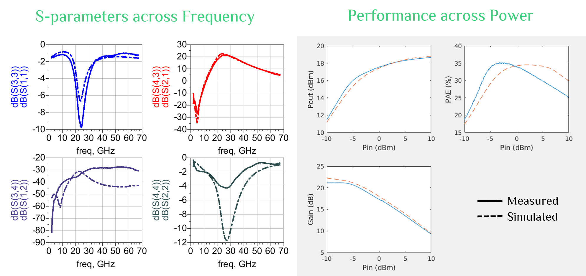
This is how it looked like in measurement:
- Overall, very good correlation between simulation and measurement
- Measured input return loss and gain track simulation well. Reverse isolation and output return loss do not track that well. We think it has to do with grounding. We might not have EM simulated M1 ground plane (blue color in image above) thinking that it is big and continuous enough. So, lesson learnt: include as much routing as you can in EM sims (bias lines, nearby structures such as pads, ground planes etc.)
- Large signal performance also tracks well. We get same P1dB and max PAE. This is great.
We hope you enjoyed our mm-wave PA design tutorial. Please leave us a feedback if you find typos or mistakes.
References
[1] http://muehlhaus.com/wp-content/uploads/2011/07/Sonnet-Ports-RFIC.pdf
[2] http://www.sonnetsoftware.com/support/downloads/manuals/st_users.pdf
[3] http://literature.cdn.keysight.com/litweb/pdf/5989-9594EN.pdf
[4] http://rfic.eecs.berkeley.edu/~niknejad/ee242/lectures.html
[5] https://www.microwaves101.com/encyclopedias/load-pull-for-power-devices
Appendix
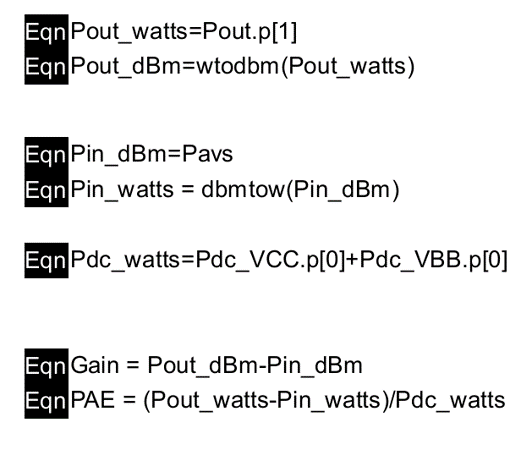
Equations for Harmonic Balance Plots:
Browse by Tags
Author: RFInsights
Date Published: 29 Dec 2022
Last Edit: 02 Feb 2023