Device Physics Explained: Key Concepts for IC Designers
Chp. 6: The Invention of the Transistor: A Step-by-Step Breakdown
6.1 The Pre-Transistor World: Setting the Stage
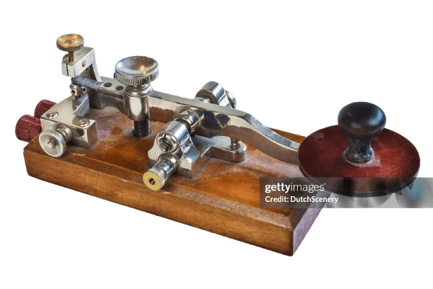
6.1.1 Relays: The First Electronic Switches
The relay was invented by Joseph Henry in 1835. It was the first electronically controlled switch. An electromagnet was used to move one piece of metal on a spring into contact with another piece of metal. A small amount of power in the magnet circuit could control a larger amount of power in the contact circuit (thus, serving as an “amplifier” as well). The device was simple, rugged, and quite reliable – an excellent switch used in telegraphs (the first system sending electric signals across wires!). The limitation was that relays moved at “mechanical” speeds – it took about a thousandth of a second to open or close the contact. It was a million times slower than its competitor, the vacuum tube.
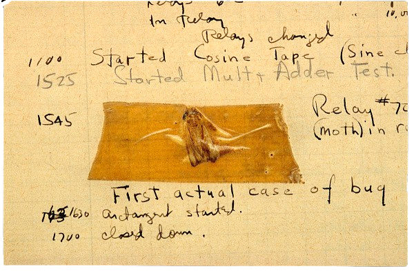
Fun Fact: The Original “Computer Bug” Was a Literal Moth! 🦟
In 1947, some folks at Harvard University were working on the Mark II computer, an early electromechanical computer. When it suddenly malfunctioned, they discovered a moth trapped in one of its relays. They taped the insect in their logbook and labeled it “first actual case of bug being found.” This popularized the term “debugging” among programmers which we IC designers seamlessly picked up. By the way, the moth’s remains are still preserved at the Smithsonian Museum! [1].
6.1.2 Cat’s Whisker Diode: The Quirky Grandparent of Semiconductors
It was known that metal-semiconductor junction behaved very weird. When a metal touched a semiconductor crystal, sometimes it conducted in one direction (acting as diode) and sometimes it conducted both ways (ohmic contact) – not known why. There was little demand for rectifiers outside of power applications, therefore semiconductor diode did not pan out much.
Then comes 1901, Marconi invents radio, and the search for “detector” or “demodulator” ignites. In 1904, just when vacuum tube diode was proposed, a very first practical semiconductor diode also emerges called as “Cat’s Whisker Diode” aka point-contact diode. The idea was same as people had observed before: touch a sharp metal wire (as thin as a Cat’s Whisker) to a semiconductor material, you will get a rectifier which can be used to demodulate AM radio signals. These detectors dominated in early radio receivers (1910-1920s) because they were cheap and required no power!
However, Cat’s Whisker diodes were too quirky! Listeners had to adjust the whisker’s contact point to find “hot spots” where rectification occurred. If you didn’t hit the right spot, or you didn’t apply the right pressure, the contact would become plain ohmic, conducting in both directions and failing as a rectifier. This inconsistency ultimately led to their downfall. By the 1920s, vacuum tubes took over, offering superior and reliable performance. However, what Cat’s Whisker diode had done was to show the world the potential of semiconductor for electronics.
.jpg)
6.1.3 Vacuum Tubes: Hot, Hungry, and High-Maintenance
While working light bulbs, Edison had noticed that electrons (then unknown) flowed from the bulb’s heated filament to a nearby metal plate inside the vacuum when the plate was positively charged. This unidirectional current flow was scientific curiosity to Edison, but he did not develop it further into any application. He got his patent and moved on.
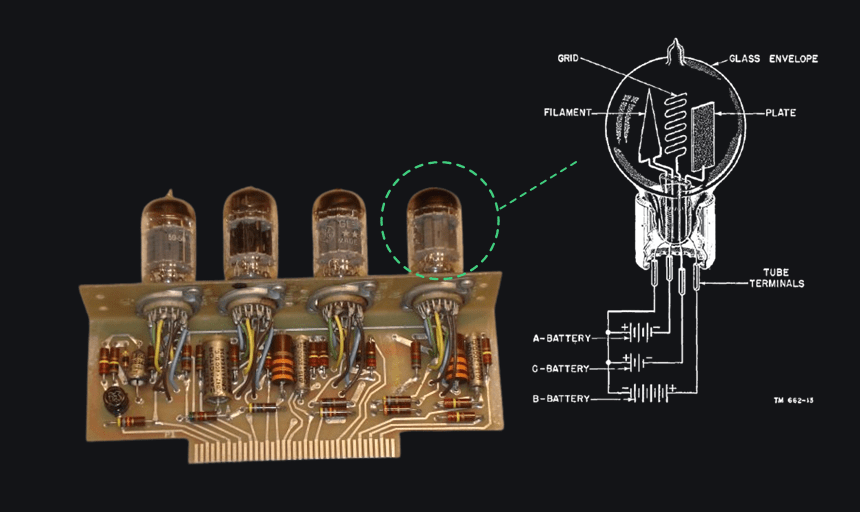
Fleming, however, figured out that “Edison effect” can be used for rectification and goes on to invent the vacuum tube in 1904. Two electrodes in vacuum with first electrode heated (cathode) and other positively charged (anode). Electrons flowed only from cathode to anode, thus vacuum tube serving as a diode. Two years later, De Forest added a third electrode “control grid” to Fleming’s diode, creating a triode. The idea was that small voltage on grid could control the flow of electrons. This vacuum tube triode could switch and amplify, and since electrons can travel at high speed in a vacuum, it was very much faster than the relay. But the vacuum tube used considerable standby power, and its lifetime was limited. The filament would burn out and the tube would fail. Thus, the vacuum tube was fine in applications where only a few were needed, such as in radios. Where thousands were needed, as in computers, the vacuum tube could not hack it [2].
So not radios, but computers gave birth to the transistor — RFIC designers, we were just along for the ride.
6.1.4 Trial, Error, and Eureka: Lessons from Creative Failures
There existed a large body of empirical knowledge of semiconductor devices based on experience with diodes for detection of radio signals. There was much art, much tinkering, but little engineering understanding and almost no science. The first half of the 20th century was an era of “creative failures” (a term coined by Shockley himself [3]), where inventions emerged from trial, error, and observation rather than deep theoretical foundations. Things were discovered first and understood later.
As IC designers, we often find ourselves in the same cycle—designing first, only to later grasp how it truly worked, lamenting our technical inadequacies. But don’t despair. Many of the greatest minds in history also followed the path of “design first, theorize later.” Check this:
Doping was Discovered, Not Invented 🤷🏽
The concept of doping emerged from early observations that certain impurities drastically changed the conductivity of semiconductors. In the case of germanium, it was Theuerer who first identified the presence of phosphorus as an n-type agent as a result of smelling traces of phosphine during ingot preparation. This led to systematic studies where elements like phosphorus or boron were deliberately introduced, leading to the discovery of N-type and P-type behavior.
PN Junction was Discovered, Not Invented 🤷🏽
PN junctions were first observed accidentally in semiconductor ingots formed by melting and refreezing high-purity silicon. During the cooling process, impurity segregation sometimes resulted in adjacent regions having different doping types, forming natural PN junctions. When researchers measured their conductivity, they found rectification—current flowing more easily in one direction than the other. This observation led to the controlled development of PN junctions and the foundation of semiconductor devices.
BJT was Discovered, Not Invented 🤷🏽
BJT itself was accidentally discovered while Shockley (and his group) were trying to make an FET work, and its theory was understood much later. However, one should note that “accidents favor prepared minds”—this breakthrough didn’t occur out of nowhere but emerged from a path filled with creative failures.
“I think one of the things that is least effective in encouraging creativity is to give the impression that students so often get in the school is that all of the nice things important things are found out nicely and neatly…most of these (inventions) require many failures to accomplish…but if one is taught that everything is neat and orderly and one never gets into a mess when trying to do something new, then you will be so conservative that I don’t think you will break new ground.” William Shockley [4]
6.2 Journey to Innovation: Birth of the Transistor
During WWII, radar systems demanded high-frequency detectors for microwave signals. Vacuum tubes struggled at these frequencies, leading to the revival of point-contact diodes made from purified silicon or germanium. Folks were done with vacuum tubes and desperately looking to make an amplifier from semiconductors.
6.2.1 Field-Effect Transistor (FET): The Early Quest for Semiconductor Amplifier
The early concepts of semiconductor amplifiers were based on field-effect mechanisms, similar to the operation of relays and vacuum tubes. Relays used magnetic fields to move mechanical contacts, turning a switch on and off. Vacuum tubes used electric fields to accelerate or repel electrons from a heated cathode filament to an anode plate, effectively switching the flow of current. Why not apply the same idea to semiconductors? Pass an electric field through the surface of a semiconductor. This field would attract or repel charge carriers within the semiconductor, forming a conductive channel near surface. Typically, this field was created by applying a voltage to a metal plate near the semiconductor’s surface. By modulating the voltage on the plate, one should be able to control current flow through the semiconductor. The first documented attempt at creating such a device was made by Lilienfeld in 1925 [5]. However, his efforts failed, as the semiconductors available at the time were not pure enough to behave as the theory predicted (and surface states were not discovered yet).6.2.2 Shockley’s First Foray: Chasing the Field-Effect Dream
William Shockley – an MIT PhD, an obnoxious but brilliant physicist working at Bell labs – had similar ideas of using field-effect to make a semiconductor amplifier while studying copper-oxide (CuO) rectifiers.
“I recognized that possibilities of amplification were inherent in Schottky’s depletion layer. The space-charge layer that spreads more deeply into the semiconductor as the reverse potential on the rectifier is increased. I saw that this spreading could be used as a kind of valve action so as to control conductivity in the semiconductor at a substantial distance from the contact.” William Shockley [3]
Shockley started such experiments in 1939, but they all failed. Then came WWII and he got separated from solid-state physics research. During that time, semiconductor technology markedly advanced, stimulated by the need Cat’s whisker diodes for radar. Bell Laboratories actively contributed to detector development, while materials were improved by the metallurgical work at the Murray Hill Laboratory.
6.2.3 Shockley’s Second Shot: Renewed Field-Effect Ventures
Post WWII, Bell Labs decided to focus on single atom semiconductors like Si and Ge and do away with complex semiconductors like CuO. Shockley attempts to make an FET again using Si this time. He attached a 90V battery to a piece of Si, puts it in the presence of electric field to attract free electrons near the edge, hopping they would create a conductive channel. When he ran the experiment, however, he was unable to detect a result. “Nothing measurable,” he explained. “Quite mysterious”.
“My calculations showed that very substantial modulation of the resistance should occur, but no effect was detected. I concluded from this research that the effects were at least 1500 times smaller than theoretically expected – clear evidence that something was the matter and that we did not have an adequate scientific understanding of certain basic phenomena that were connected with field-effect amplifying devices.” William Shockley [3]
6.2.4 Bardeen Explains “Surface States” Blocked Electric Field
John Bardeen, who had just finished his PhD at Princeton on Quantum physics, joins Bell labs under the invitation of Shockley. Shockley asked him to check the validity of his calculation to understand the failure of his experiments. Bardeen confirmed, about two weeks later, the accuracy of Shockley’s calculations and was equally puzzled by the discord between theory and experiment. Bardeen’s research leads him to propose that these experiments failed because the electric field was not penetrating the body of the semiconductor material but was terminated by immobile charges trapped at the semiconductor surface because of dangling bonds. He called them “surface states” and said that these blocked the external field at the surface and, thereby, shielded the interior of the semiconductor from the influence of the positively charged control plate.

6.2.5 Brattain Validates the Surface State Puzzle
According to Bardeen, the surface of the semiconductor might be so charged as to repel majority carriers. For example, for a p-type silicon specimen, a positive surface-state charge would repel holes, the majority carriers in the specimen. If photons of light fall on the semiconductor and generate hole-electron pairs, then the field just below the surface (created by these immobile charges) will separate them, electrons going to the surface and holes to the interior, this separation causes the surface potential to become more negative. Measurement of surface potential actually being negative, when light was shone on semiconductor, indeed validated surface state theory. Such photovoltaic experiments were being actively run by Walter Brattain (an experimental physicist who worked with Bardeen) at Bell labs [3].
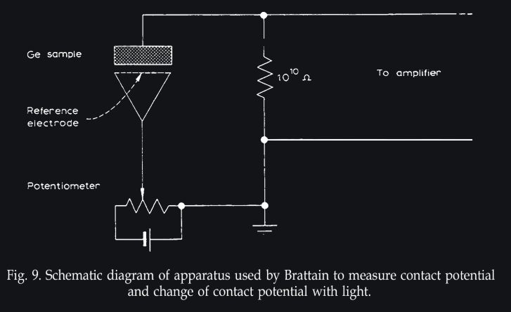
6.2.6 Gibney’s Strategy to Outsmart the Surface States
Gibney, a physical chemist recruited by Shockley to round out the expertise of semiconductor group, made the key suggestion that voltage be applied between the metal plate and the semiconductor while both were immersed in an electrolyte. Electrolyte would become polarized under electric field and if polarization is such that it assisted the surface states, this would further increase the negative potential. And that is what happened, when Brattain dumped his whole experiment into electrolyte, he measured larger negative potential. This means the surface state effect increased. If it can be increased with this polarization, one should be able to completely remove it the opposite polarization. That was it! Thus, for the first time, there was some understanding of the persistent failure to observe the field effect and an opportunity to intervene [2].
“This new finding was electrifying. At long last, Brattain and Gibney had overcome the blocking effect of the surface states—the practical problem that had for so long caused the failure of our field-effect experiments.” William Shockley [3]
6.2.7 From Theory to Practice: Harnessing the Field Effect
When Bardeen was told what had happened, he suggested a new geometry to produce an amplifier. By now they had understood that not only can one overcome surface states but also modulate conductivity by attracting or repelling majority carriers on the edge of surface, but one can also do opposite that is to attract minority carriers on the surface which they thought can be controlled better.
Bardeen suggested to place a drop of electrolyte (water in this case) on a piece of Si. Coat a metal wire with wax to insulate it from the electrolyte, then push it through the drop to contact the Si surface. Take another wire and make contact with water (not Si). Potentials would be supplied between the water and the Si, and also between the wax point and the Si. They made point contacts in hope to better understand surface states by localizing the interaction. The goal was to adjust the Si conductivity by adjusting potential on the contact touching the water. A very similar experiment like before, just done in a very localized controlled way, and instead of checking conductivity modulation across the surface, this time they were testing it through inversion layer (means layer of minority carriers — because they are “inverted” in polarity as compared to bulk which consists of majority carriers).


“It was found that the magnitude of this current could be changed by applying a voltage on the electrolyte probe, and thus, by the field effect, changing the conductance of the inversion layer. Since under static conditions only a very small current flowed through the electrolyte, the set-up could be used as an amplifier.” John Bardeen [9]
Once they’d gotten some amplification, they started playing with materials and electrolyte to increase amplification. Bardeen suggested they replace the silicon with germanium. They got a current jump, all right — an amplification of some 330 times [6]. But there were several problems. The water evaporated too quickly. So, they changed the electrolyte to glycoborate, which evaporates very slowly. This worked quite well. But the device would not amplify above 8 cycles per second. They were quite sure that the electrolyte was responsible for the slow response [7].
6.2.8 Liquid No More: Transitioning to Solid-State Solutions
Liquid electrolyte had proven their theory of surface states and even got them the first working semiconductor amplifier! They filed the first patent on transistor. However, they were not quite there yet. Liquid is liquid. How can you make an amplifier completely out of solids? They wondered same and suggested that solids could be used in the concluding sentence of their first transistor patent [8]:
“It is of course evident that the liquid dielectric could be replaced by a solid dielectric if one can be found having the proper ionic mobility to form such a dipole layer at the surface of the semiconductor [8]“
6.2.9 Accident Favor the Prepared Minds
Bardeen had observed rust growing on Ge surface which was actually Germanium Dioxide (a solid dielectric!). What better dielectric could they have used other than one which naturally grows on it? So, they decided to replace water with Germanium Dioxide. Gibney prepared a special slab of Ge with a shimmering green oxide layer on one side. Brattain began to insert the point contacts. It worked, and it worked too well! It worked as if there was no oxide layer at all. As Brattain poked the contacts in again and again, he realized that’s because there wasn’t an oxide layer at all. He had washed it off by accident. Brattain was furious with himself but decided to fiddle with the point contact anyway. To his surprise, he actually got some voltage amplification — and more importantly he could get it at all frequencies! [6]
“The effect was large enough to give some voltage, but no power amplification.” John Bardeen [9]
6.2.10 Point-Contact Transistor is Born
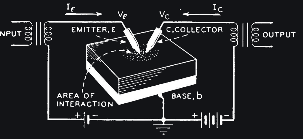
Bardeen and Brattain had discovered by now that the amplification was not happening much in the way they thought (field effect mechanisms) but somehow through injection of carriers directly into the semiconductor when the metal contact accidentally touched the surface. They thought that metal contact injected (minority carriers) holes, which flew through (n-type) Ge surface and reached other point contact to enhance its current although this is not exactly what happened and correct theory was understood much later when Shockley developed theory of PN junction and minority carrier injection. Anyway, this was their understanding at that time, and this is what they published too [10].
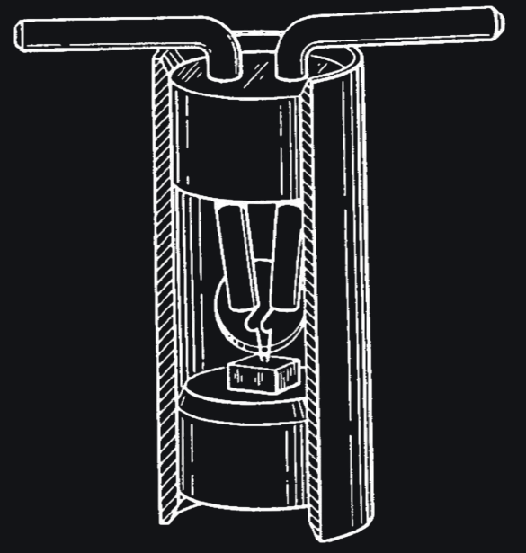
Now to get some power gain they thought of bringing point contacts as close as possible. To do that, contacts were made by evaporating gold on a plastic wedge and then separating the gold at the point of the wedge with a razor blade to make two closely spaced contacts. The whole triangle was then held over a crystal of Ge on a spring, so that the contacts lightly touched the surface (that is why the first transistor looks very weird when you look at its picture – plastic wedge, springs, thin wires, slab of Ge etc.). When they ran this experiment, they were able to get 20dB power gain [9]. Voila, that was it. Point-contact transistor is born. Theory maybe incomplete or wrong but at least they had built something that worked! This was December 16, 1947. Folks at the lab called it “magnificent Christmas present”. Bell labs soon began arranging a patent application for this new device [11].


6.3 Beyond the Breakthrough: The Transistor’s Lasting Legacy
6.3.1 The Big Reveal: Taking the Transistor to the World
When Bell Labs held a press conference in June 1948 to announce that its scientists had invented transistor, it wasn’t easy to understand why these wired blocks of semiconductor merited a special announcement. The New York Times buried the story on page 46. Time magazine did even better, reporting the invention under the headline “Little Brain Cell” [13]. However, they did make it to the cover of electronics magazine — at this time the name of the invention wasn’t quite decided yet, and it was called “Crystal Triode” (word “triode” taking inspiration from vacuum tube triode)
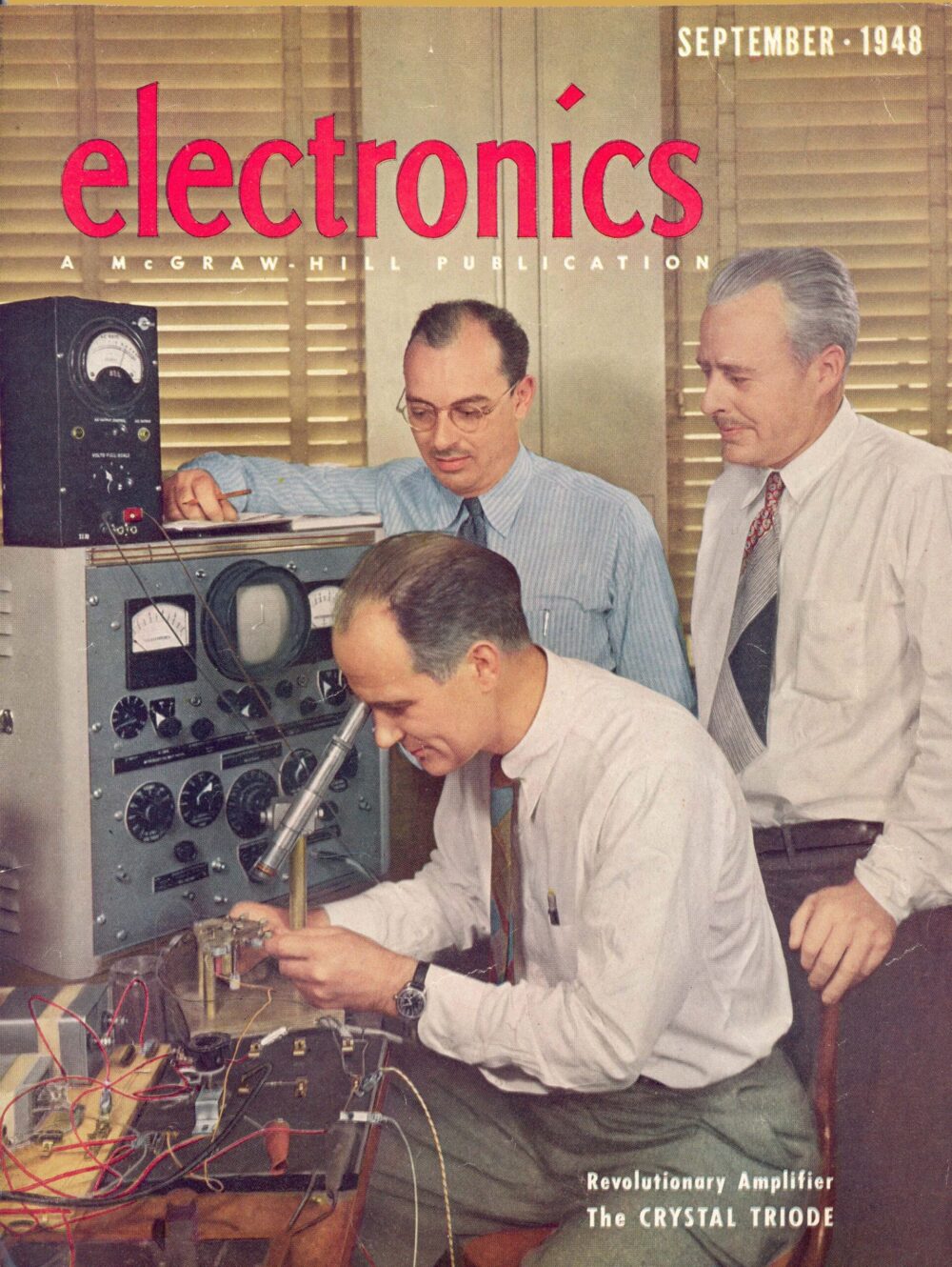
PS: Walter Brattain hated this picture. Bardeen was asked why not? and he shook his head saying no “that’s Walter equipment and our experiment in the building does not have anything to do with it” [15]
6.3.2 Naming the Revolution: The Birth of the ‘Transistor’
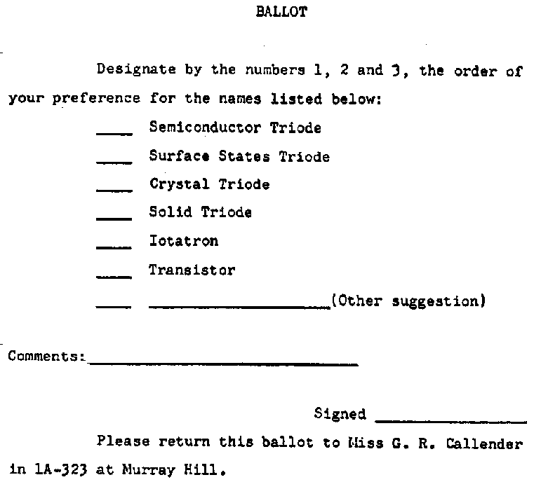
It had become increasingly clear that this particular invention really needed a great name. The descriptive terms that were floating around in lab were “Semiconductor Triode” and “Solid-state Amplifier” just wouldn’t cut it. One guy came up with the name “Transistor” based on the abbreviations “transfer” and “varistor” because this device really behaved like a transfer variable resistance that is by applying a variable potential at one contact you could transfer variable resistance to other contact. However, the final name was to be decided by a committee, and it failed to reach a unanimous decision. So, the name was opened up to a vote. Engineers at lab received a ballot as shown in image. The name transistor won by a landslide. You can read the entire memo here.
6.3.3 Shockley’s Discontent: A Clash of Visionaries
When Bardeen shared the news point-contact transistor discovery with Shockley, Shockley was stunned. He was enormously frustrated by the fact that Bardeen and Brattain had found it on their own without any direct involvement of him. He wanted to play a more significant personal, rather than managerial, role in what was obviously a development of enormous potential importance. He also took over and asked Bardeen to work on this and this and stay away from that as that is his territory [15]. Bardeen was very angry, but he was not quick-tongued. Eventually, he decided to leave Bell labs. Shockley once said in an interview:
“If someone had simply studied electrical properties of two points brought close together on a semiconductor, it’s quite possible transistor might have been invented back in 1915.” William Shockley [4]
6.3.4 Shockley’s Hotel Room Rampage: Birth of the Junction Transistor
Shockley was furious that his colleagues had discovered an experiment to prove his theories, and he was committed to outdoing them.“I experienced frustration that my personal efforts, started more than eight years before, had not resulted in a significant inventive contribution of my own.” William Shockley [3]
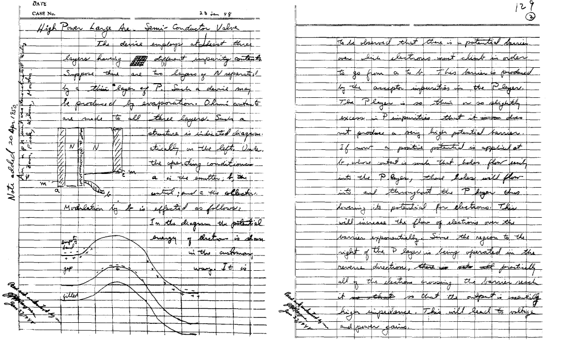
He locked himself in Chicago hotel room for two weeks over Christmas and began imagining different transistor structures, based on his unparallelled understanding of semiconductor physics [13]. By late January 1948 Shockley had figured out the important details of his own design. His approach would use a three-layer sandwich of semiconductor material — silicon or germanium — with wires attached at each end and in the middle, to an inner “base” layer. He eliminated the two fragile “point contacts” of Bardeen and Brattain’s unwieldy contraption, which would make manufacturing difficult and lead to quirky performance. Based on the boundaries or “junctions” between the layers; to be established within the semiconductor material itself, his amplifier should be much easier to mass-produce and far more reliable.
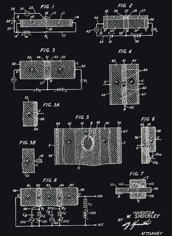
It still took more than two years before other Bell researchers perfected the techniques needed to grow ultrahigh-purity germanium crystals with just the right characteristics to act as transistors and amplify electrical signals. On the 4th of July 1951, Bell Labs announced the production of the first “bipolar junction transistors,” which had been successfully fabricated by chemists Morgan Sparks and Gordon Teal based on Shockley’s designs [12].
Next, let’s put ourselves in the shoes of Shockley and understand how he could have come up with the concept of BJT.
Appendix
How Did the Point-Contact Transistor Really Worked Though?
Although originally intended as a field-effect device, Shockley’s later work on NPN transistors revealed that the point-contact transistor operated on similar principles. In these early experiments, the metal contact inadvertently oxidized the semiconductor surface, creating a thin p-type region within the n-type bulk. This accidental p-n junction effectively formed an NPN transistor. For more details, check this out.
References
[1] Grace Murray Hopper,”The First Bug,” Annals of the History of Computing, vol. 3 #3, 1981, pp. 285-286.
[2] I. M. Ross, “The invention of the transistor,” in Proceedings of the IEEE, vol. 86, no. 1, pp. 7-28, Jan. 1998, doi: 10.1109/5.658752
[3] W. Shockley, “The path to the conception of the junction transistor,” in IEEE Transactions on Electron Devices, vol. 31, no. 11, pp. 1523-1546, Nov. 1984
[4] William Shockley Interview, 1969
[5] 1926: Field Effect Semiconductor Device Concepts Patented
[7] The Genesis of the Transistor, with Bonus Introduction – AT&T Archives
[8] Three-electrode circuit element utilizing semiconductor materials
[9] Semiconductor Research Leading to the Point Contact Transistor
[10] J. Bardeen and W. H. Brattain, “The Transistor, A Semiconductor Triode,” in Proceedings of the IEEE, vol. 86, no. 1, pp. 29-30, Jan. 1998
[11] Three-electrode circuit element utilizing semiconductive materials
[12] Crystal Fire: The Invention, Development and Impact of the Transistor
[13] Chip War: The Fight for the World’s Most Critical Technology
[14] Electrons and Holes in Semiconductors: With Applications to Transistor Electronics
[15] Spark of Genius: The Story of John Bardeen
[16] Circuit Element Using Semiconductive Material – Filed on June 17, 1948, now U.S. Patent No. 2,524,035.
Browse by Tags
RFInsights
Published: 03 Mar 2025
Last Edit: 03 Mar 2025