Device Physics Explained: Key Concepts for IC Designers
Chp. 7: How Does a BJT Work?
7.1 The Road to Innovation: How Does a BJT Work?
The path to creativity is neither easy nor direct. The idea of junction transistor appeared so obvious to Shockley only after he had invented it. It had eluded him so many times. It was only after when point-contact transistor had born and folks at Bell Lab had realized a transistor could be made with carrier injection (rather than field-effects), Shockley connected the dots and finally came up with the idea of bipolar junction transistor. It was Shockley’s persistence that even made one of his colleagues suggest that he should name transistor as “persistor“.
Shockley himself explained his journey [1]:
“My hope is that by being frank about my own limitations in seeing what later seemed so obvious, I may encourage my readers to persist rather than give up when they feel distressed over their own limitations.” William Shockley [1]
Let’s step into Shockley’s shoes and re-invent the transistor—discovering how does a BJT work from first principles.
7.2 Reinventing the Bipolar Junction Transistor
Let us travel back in time to Christmas of 1947—the point-contact transistor has just been invented, and intense experimentation at Bell Labs has revealed a critical insight: if you inject minority carriers into a semiconductor, you can achieve amplification. But how does it work?
Bardeen has his surface-state theory, attributing the effect to conduction along the semiconductor surface. However, we—standing in Shockley’s shoes, locked away in a hotel room—are skeptical. There must be something deeper at play. The key hint? Minority carrier injection. Let’s build upon it to understand how does a BJT work.
7.2.1 Control Over Minority Carrier Injection
We know that when a PN junction is forward biased, electrons are injected from the n-side and cross the depletion region into the p-side. Since these electrons are minority carriers in the p-side, they diffuse the heck out reaching to the contact at p-side, thus completing the loop, flowing back to the applied voltage source. Similarly, holes injected from the p-side into the n-side behave the same way. Fair. That explains the how current flow in a PN junction.
But where is the amplification?
The magic lies in the fact that minority carrier injection increases exponentially with the applied voltage. This means we have an intrinsic voltage-to-current (V-to-I) exponential relationship—a crucial ingredient for amplification. Now, the challenge becomes: how do we collect these carriers efficiently (instead of letting them diffuse back to the applied voltage source)?

7.2.2 Employing a Reverse-Biased Junction for Carrier Collection
Let’s brainstorm. What’s a good way to collect minority carriers? Specifically, how do we collect electrons from the p-side? Simply adding another contact would allow holes to flow too, splitting the current. That’s not the answer.
What we really need is an electric field—a force that can sweep carriers in the right direction. Holes move with the field, electrons against it. Since we want to take electrons out of p-side, we need an electric field directed toward the p-side. But how do we introduce such a field inside a semiconductor?

PN junctions! They naturally create built-in electric fields. So, let’s place another PN junction next to the first one. To pull electrons from the p-side, the new junction’s field must point toward it. This means we should reverse bias the junction, and this reverse bias would not inject minority carriers of its own (because that happens in forward bias), so this should be able to collect electorns. This is all making sense.
Here’s why: In a reverse-biased PN junction, the depletion region acts like a vacuum for minority carriers—sweeping them away instantly. The concentration of minority carriers near the edges of the depletion region is practically zero, meaning any electron that gets close is immediately pulled across. Well, this is very efficient collection!
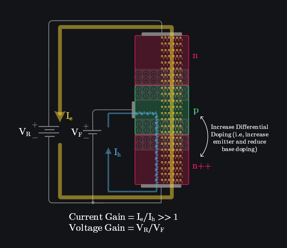
An interesting insight: The forward-biased supply (\(V_F\)) is not actually injecting the electrons now, it is merely controlling the injection. Infact, electrons are injected by the reverse bias supply (\(V_R\)). That’s how the loop will complete: if a supply is collecting something, it must be injecting same thing, because current through both terminals of supply must remain same.
But what about gain? The current gain here is just 1! I mean all we did was to collect electrons. There was no amplification here. However, we did get something: voltage gain. Since the reverse bias voltage can be arbitrarily high (eventually limited by breakdown), we can achieve significant voltage gain \(\frac{V_R}{V_F}\).
Phew! At least we got something. Now, let’s work on achieving current amplification.

7.2.3 Optimizing Doping and Geometry for Gain
We didn’t get current gain because electron and hole currents were roughly equal. But what determines these currents? Doping. We implicitly assumed similar doping levels for the n-side and p-side (along with similar diffusion and mobility). Think about it: if more carriers are available, more will be injected for a given bias. So, all we need to do is heavily dope the n-side emitter to inject more electrons and lightly dope the p-side to inject fewer holes.
- Heavily dope the n-side emitter (increases available electrons)
- Lightly dope the p-side (reduces hole injection)
This deliberate imbalance ensures that the hole current (supplied by \(V_F\)) remains small, while the electron current (collected by \(V_R\)) is significantly larger. This is the secret behind achieving current amplification—answering one of the most crucial parts of how does a BJT work.
And there we have it! By strategically placing two PN junctions and tuning the doping levels, we’ve built a bipolar junction transistor that delivers both current gain and voltage gain. How wonderful!
But what about collector doping and the impact of geometry on performance? We’ll explore those details in the next post.
7.3 From Theory to Reality: How Engineers Made the BJT Work
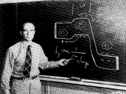
Theory is one thing, but making it work in practice is another. Growing clean PN junctions and precisely controlling impurities was no simple feat. Transforming Shockley’s theoretical concept into a practical device was an engineering challenge. Engineers faced obstacles in materials processing, fabrication, and reliable performance. It wasn’t until the spring of 1950 that a satisfactory realization of the junction transistor emerged, with real excitement building by early 1951. This evolution from theory to working device epitomizes the difference between scientific insight and engineering execution.
As William Shockley put it [1]:
“A satisfactory realization of the junction transistor was not achieved until the Spring of 1950 and real excitement about it did not develop until early 1951. I believe that my facial expression in Figure expresses my attitude towards the disappointments that characterized the “persistor” period of late 1949 and early 1950.”
Understanding how does a BJT work goes beyond semiconductor physics—it’s about solving real-world engineering challenges to turn theory into revolutionary technology. But for now, let’s put on our physicist hats and focus on the device physics fundamentals. In the next post, we’ll dive deeper into the intricate details of BJT operation. Stay tuned!
FAQ
Q: Why is a junction transistor called a “Bipolar Junction Transistor (BJT)”?
A: Is it because it has two junctions with opposite polarities—one forward biased and the other reverse biased? Nope. The real reason is that both electrons and holes participate in current flow. In contrast, Field-Effect Transistors (FETs) are unipolar because their conduction relies on only one type of charge carrier—either electrons (n-channel) or holes (p-channel).
Q: Why do we call it “minority” carrier injection? What about majority carriers? Can they be injected?
A: We focus on minority carrier injection because that’s where the real action happens—leading to huge diffusion currents. Now, imagine injecting holes into a p-type material. What happens? Not much. Holes are already in high concentration there, so the concentration gradient (which drives diffusion) is weak. Plus, a reverse-biased PN junction won’t be able to sweep them across—it only collects minority carriers efficiently. That’s why injecting minority carriers is the key to making devices like BJTs work!
References
[1] W. Shockley, “The path to the conception of the junction transistor,” in IEEE Transactions on Electron Devices, vol. 31, no. 11, pp. 1523-1546, Nov. 1984
Browse by Tags
RFInsights
Published: 10 Mar 2025
Last Edit: 10 Mar 2025