Linearity Improvement Techniques for on-chip Amplifiers
The Fantastic Four of Linearity Improvement Techniques
Linearity is one of the most, if not THE most, important metric in circuit design. All analog circuits are inherently non-linear mainly because of non-linear behavior of transistors. Many linearity improvement techniques have been discovered or invented in literature yet we only see a few of them in industry practice. This article discusses those few yet fundamental linearity improvement techniques that you must try before you go on with any advance niche solution.
Context
Let’s discuss these techniques in context of V2I converter. A V2I converter or GM cell converts voltage to current, and is usually found in all kind of circuits. For example, it is an essential block in an active mixer based TX as shown in image below. It takes voltage signal from baseband filter (BBF), converts it to current to feed into Gilbert Cell Mixer.
Ok, so say we want to build a linear V2I converter. Let’s start with transistor itself. It’s a natural V2I converter. What’s wrong with it? First off, its gm is a function of signal swing, higher swing leads to higher gm. We want gm to remain fixed over signal swings. Secondly, it does not have any common mode rejection (CMRR). Any variation in DC bias with process or temperature will change the gm. We can resolve this by adding a tail current source. Ok, but how do we fix linearity? We know a resistor is a linear V2I converter, you drop any voltage across it and it produces proportional current (Ohm’s law). It would then be ideal if we could use a resistor for V2I conversion? Yes, but unfortunately there is no direct way we could use a resistor (try to think of a way). First of all, previous stage would need to drive very hard if we put a small resistor, and if we put a big resistor then gm would be pretty low (that would mean its more like a attenuator then amplifier, which is a bummer). Secondly, we need a way of copying current passing through this resistor and feed it to the mixer. It is for latter that we need something more than just a resistor for V2I conversion, and that something more could be a transistor. So that is what folks did. They connected a resistor to a transistor and called it resistive degeneration. The idea is to pass all the voltage at the gate of transistor to the resistor, resistor would convert it to current (which would be very linear), and then transistor can pass that current to the mixer. This works well if the loopgain (gmR) is very very high, otherwise transistor has difficulties passing all the voltage to resistor and drops some voltage across its gate to source (which of course again is function of signal swing, anything with transistor is a function of signal swings really!). But you got some linearity by just using a resistor and transistor, not bad at all. This is where textbook usually stops, and this is where we begin.
The Fantastic Four
There are four basic linearity improvement techniques that are shown in “infographic” below.
1. FeedBack
Realizing the problem with resistive degeneration was limited loopgain (gmR), one can try to fix it by increasing gm of transistor since we wouldn’t want to change R as it determines our V2I gain. gm can be improved by increasing current of transistor (which is a no no, high current comes with so many issues, not just the power consumption but bigger devices, thicker routing lines, bigger ground bounces, bigger dc offsets, higher noise of bias currents etc.). There are other ways of improving the gm, one of which is called feedback. The idea is to place an opamp before transistor and close the loop on source node of transistor as shown in image below. Opamp would try to force same voltage at its +ive and -ive terminal thereby making the voltage at source node of transistor equal to the input voltage. Voila! this is what we wanted, to pass all the input voltage to resistor. Another way of seeing this is as if transistor gm got boosted by gain of opamp, therefore we also call this linearity improvement technique as gm boosting [4].
2. FeedForward
Another way of boosting transistor gm is positive feedback. We hear all the time how bad positive feedback it, it make your system oscillate and all that, which is true but its very nature of oscillation (= infinite amplification) can be used to boost gm if employed properly. Caprio’s Quad [3] is one such example as shown in image below. A cross coupled differential pair is introduced between main transistor and degeneration resistor. A cross couple pair has \(\frac{-2}{g_m}\) impedance looking into it which adds to transistor’s gm nulling out the overall gm, and thus variations. Since signal is first fed to main transistor and then feedback happens, this is also called as feedforward linearization.
A more intuitive way of understating it is this: Say M1 received \(V_+\) which increased the current to \(I_+\) while M2 received \(V_-\) which decreased the current to \(I_-\). Now \(I_+\) being higher current would drop higher \(V_{GS}\) across transistor, lets call it \(\Delta V_+\), whereas \(I_-\) would drop smaller \(V_{GS}\), lets call it \(\Delta V_-\). It is the variations of these \(\Delta Vs\) that create signal dependent voltage across resistor. Our goal is to make voltage (\(V_A-V_B\)) across resistor independent of \(\Delta V\) variations which cross couple pair does perfectly by cancelling these variations. Image below shows that \(V_A-V_B\) does not have any \(\Delta V\) when signal traverses the loop (from M1 to M4 to VA to VB to M3 to M2).
3. SuperPosition
The idea of superposition is simple: Add two non-linearities in hope that they cancel each other out. There are different ways this can be accomplished:
Method#1: Say if amplifier A has compressive non-linearity (meaning gain decreases with higher signal) and amplifier B has expansive non-linearity (meaning gain increases with higher signal), A+B would be linear since compression and expansion would compensate each other. Example: take a current source, bias its VDS at its knee point, now any voltage swings at drain of current source would result in expansive current (because swings will take it to triode region where gds will expand). Add this current to your main amplifier to compensate for its compressive non-linearity.
Method#2: Say amplifier A generates IM3 with some phase \(\phi\), if you could have another amplifier B which generates similar IM3 but with opposite phase \(-\phi\), A+B would be linear. This is not hard to achieve: connect two instances of an amplifier and just bias them at different points, you will already start seeing IM3s subtracting (or adding). Techniques like these are knows as derivative superposition [1].
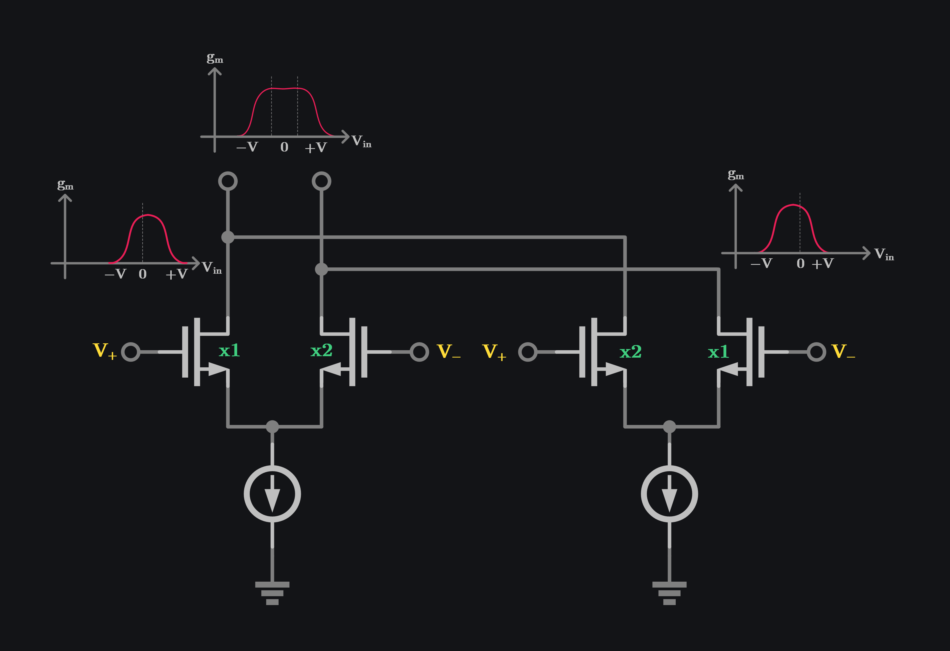
Method#3: A differential pair gm is very linear right at its bias point but then falls off quickly giving a hump like shape. Good thing is we can move the hump location by setting a different bias point or different device size between +ive and -ive transistor. This means we can take N diff pairs, offset their sizes, add their outputs, and gm would flatten, thus improving linearity. This is shown in image below where two diff pairs are taken. \(V_+\) is given to two transistor with different sizes (one is twice the size of other) and the outputs are added. Total gm can be seen to be flat over wider range of input swings.
4. PreDistortion
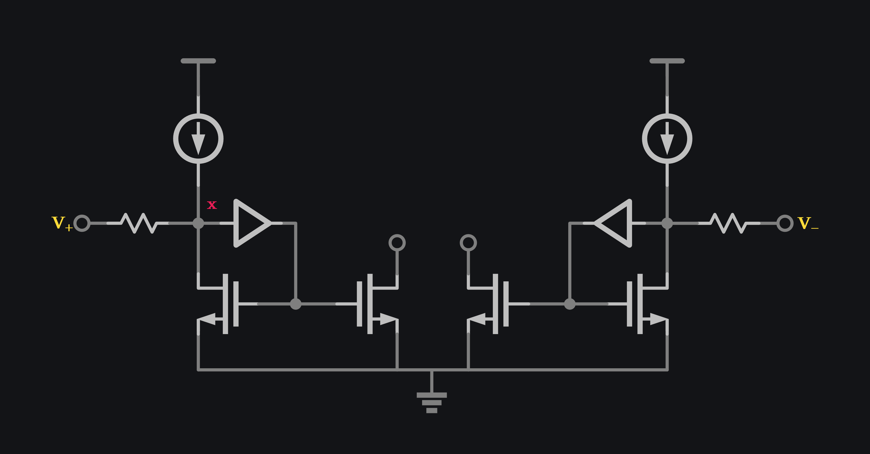
If a transistor’s V2I conversion distorts the output by squaring the signal, then same transistor’s I2V distorts the output in an inverse manner (by square-rooting the signal). This means if we cascade I2V and V2I together, the output should be linear. That is precisely what a current mirror accomplishes. You input a current to diode branch, and it gives you perfect replica of it in mirror branch. It takes the current, converts it to voltage (thus pre-distorting it by taking square root of it), that distorted voltage is fed to the mirror branch, and replica current comes out (which is clean of distortion because mirror un-distorts it by taking square of it). This is awesome, however there is a catch: it is current in and current out. We wanted voltage in and current out. We again need help of our friend resistor. We can add an opamp between drain source terminal of diode branch of current mirror as shown in the image below. The idea is to drop the impedance at node x so much that it acts as a virtual ground, this way all voltage provide by \(V_+\) drops across resistor, and current generated flows through diode transistor which is then mirrored to the output transistor. This circuit is noisy and flicker noise can be high, usually current mirror is degenerated to reduce noise transfer function to output (How? Recall why cascode noise is negligible in a cascode amplifier).
References
[1] Derivative Superposition – Control of Circuit Distortion by Derivative Superposition Method
[2] PreDistortion – The active-input regulated-cascode current mirror
[3] Caprio’s Quad – Precision Voltage to Current Converter
[4] Regulated Cascode (gm boosting) – A high-swing, high-impedance MOS cascode circuit
Browse by Tags
RFInsights
Published: 30 Jun 2023
Last Edit: 30 Jun 2023