Passive Mixers
Chp. 1: Input Impedance of Switched Resistor
In this post, we analyze the input impedance of a resistor that is periodically switched on and off, and compare it with the impedance of a continuous (unswitched) resistor. We then explore how this switching behavior enables impedance transformation, a key principle in passive mixers and switched-capacitor circuits.
1.1 When a Resistor is Switched ON & OFF
1.1.1 When Input is DC
Let’s start simple. Assume you have a 1k\(\Omega\) resistor connected to 1V DC. It would draw 1mA. What if we put a switch in-between? When switch turns ON, resistor draws current and when switch turns OFF, no current flows. Alright, now let’s say switch turns ON 50% of the time and remains OFF 50% of the time (in other words duty cycle is 50%), intuitively you would expect that since source is providing 1mA half the time and zero the other half, on average 0.5mA is drawn from the source i.e., DC current is 0.5mA. Hmm as if resistor value is doubled (meaning if there was no switch, a 2k\(\Omega\) would draw 0.5mA but now with switch even 1k\(\Omega\) is drawing 0.5mA). This means switching things ON and OFF can transform impedance. So, matching networks (Ls & Cs) are not the only way to match impedance.
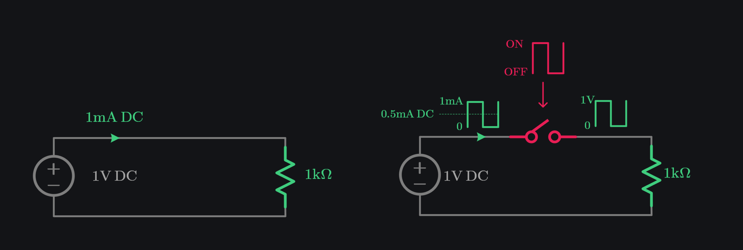
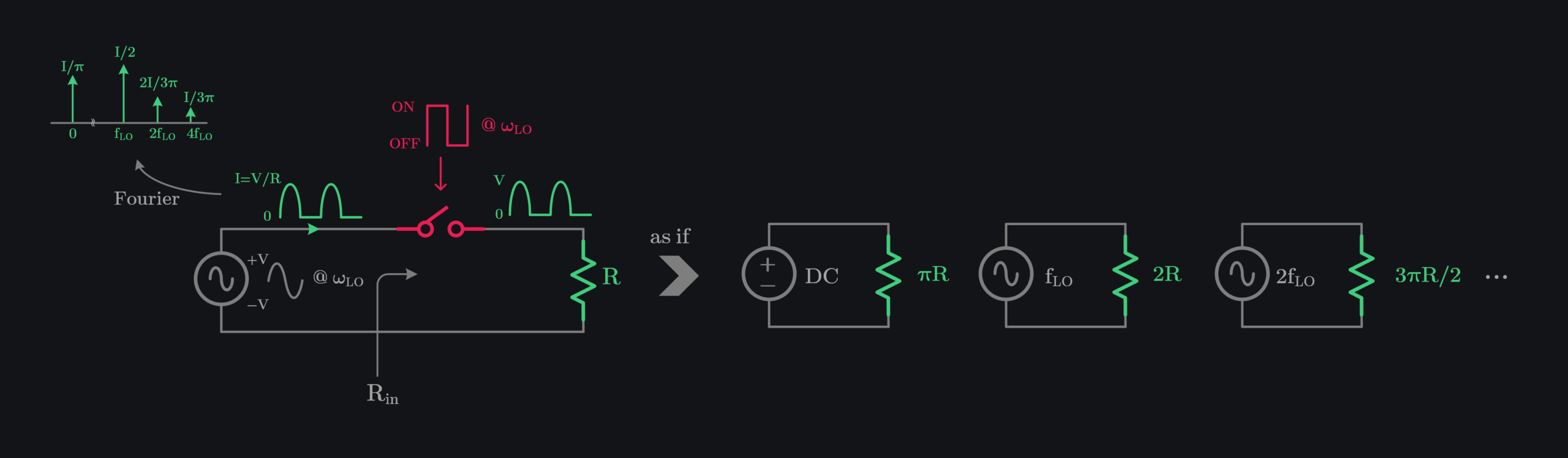
Let’s develop this mathematically. Say, switch is turned ON and OFF by frequency \(\omega_{LO}\), load is a resistor R, and source is DC with amplitude V. Current drawn from source would look like a square wave toggling between 0 and amplitude \(\frac{V}{R}\), and can be written as:
Now wait, there is something here. We see at DC current drawn is \(\frac{1}{2R}\) which matches with our intuition, but we are also drawing current at harmonics of \(\omega_{LO}\). This also makes sense since current drawn looks like a square wave and we know square wave is rich at odd harmonics. But your source in only DC, how come it can provide current at LO frequency? Simple way to think about is to imagine in time domain. In time domain, you are simply taking constant current \(\frac{V}{R}\) from source when switch is ON and 0 when OFF, that’s all source is providing.
What is of significance here is that the fact that some current being drawn at LO frequency and its harmonics means you are seeing some impedances at these frequencies. This is as if your resistor \(R\) is transformed to \(\frac{\pi}{2}R\) at \(\omega_{LO}\), to \(\frac{3\pi}{2}R\) at \(3\omega_{LO}\), and so on as per (1). Thus, we can write input impedance of a switched resistor as:
What does negative sign mean? We will answer shortly.

1.1.2 When Input is of Same Freq as CLK
Let’s break it down with another example to fully grasp the concept. Say now input is a sinusoid with frequency \(\omega_{LO}\) and amplitude \(V\), and our switch is also turning ON and OFF at frequency \(\omega_{LO}\). When switch is ON, sinusoid go through and drives resistor \(R\). When switch is OFF, no current flows. The current drawn from source will look like a switched sinusoid as shown in image below. We can model this by saying this is as if a square wave toggling between 0 and 1 multiplied with our sinusoid.
Thus, input impedance can be written as:
1.1.3 General Formula for Switched Resistor Input Impedance
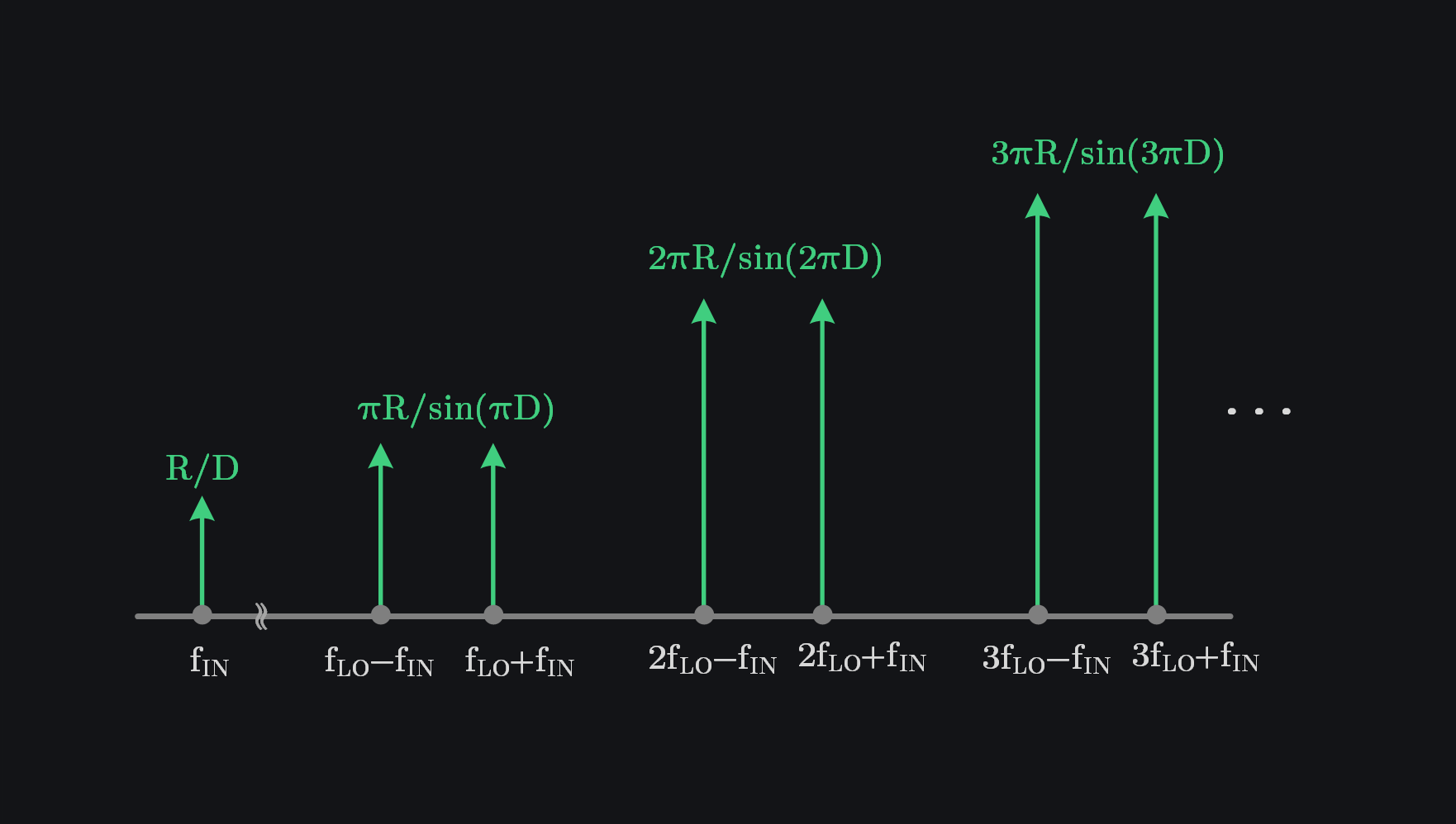
In general, for an input signal of frequency \(\omega_{IN}\) with 50% duty cycle driving a resistor R through a switch toggling at frequency \(\omega_{LO}\), we can write input resistance to be:
where,
- R transforms to 2R at \(\omega_{IN}\) because of 50% duty cycle. You are only drawing current half the time, and this makes your load look like 2x.
- Factor of \(\pi\) appears with R at \(\omega_{LO}-\omega_{IN}\) and \(\omega_{LO}+\omega_{IN}\) because fundamental coefficient of square wave is \(\frac{2}{\pi}\) which splits into sum and difference product and thus gets halved to \(\frac{1}{\pi}\). Meaning current drawn is scaled by \(\frac{1}{\pi}\) i.e., as if resistance is scaled by \(\pi\).
- Factor of \(3\pi\) appears with R at \(3\omega_{LO}-\omega_{IN}\) and \(3\omega_{LO}+\omega_{IN}\) because third harmonic coefficient of square wave is \(\frac{2}{3\pi}\) which splits into sum and difference product and thus gets halved to \(\frac{1}{3\pi}\). Meaning current drawn is scaled by \(\frac{1}{3\pi}\) i.e., as if resistance is scaled by \(3\pi\). Note the negative sign. Is it a negative resistor? Yes. Can it be used? Maybe if you get creative. Let’s say you want to use that negative part at \(3\omega_{LO}-\omega_{IN}\), so you send something at this frequency (i.e., your source is sending some signal at \(3\omega_{LO}-\omega_{IN}\) in addition to existing \(\omega_{IN}\)). Now, \(3\omega_{LO}-\omega_{IN}\) will generate its own “2R” component and that will add to -ive component generated by \(\omega_{IN}\) making the overall impedance positive again. (Note by addition we mean parallel combination since current delivered by each source is in parallel i.e., \(3\omega_{LO}-\omega_{IN}\) will deliver current in addition to existing current established by \(\omega_{IN}\))
1.1.4 Intuition Behind Switched Resistor Input Impedance
We saw that you can transform R to 2R at \(\omega_{IN}\) if you add a switch in-between and toggle it with 50% duty cycle. What if changed duty cycle to 25%? We would see 4R at \(\omega_{IN}\). This means we can transform to any higher impedance; all we need is to choose duty cycle. The reason as explained before is same, if you reduce the duty cycle, you are not drawing the current from your source all the time, this is reflected as less current drawn compared to a continuously-drawn non-switched circuit, and this less current drawn means as if load is bigger.
In general, co-efficient of square wave toggling between 0 and 1 can be given as:
where,
- D is duty cycle (e.g., 0.5 for 50%)
- n is harmonic number for n\(\ge\)1
Image below shows how your impedance will look like as a function of duty cycle.
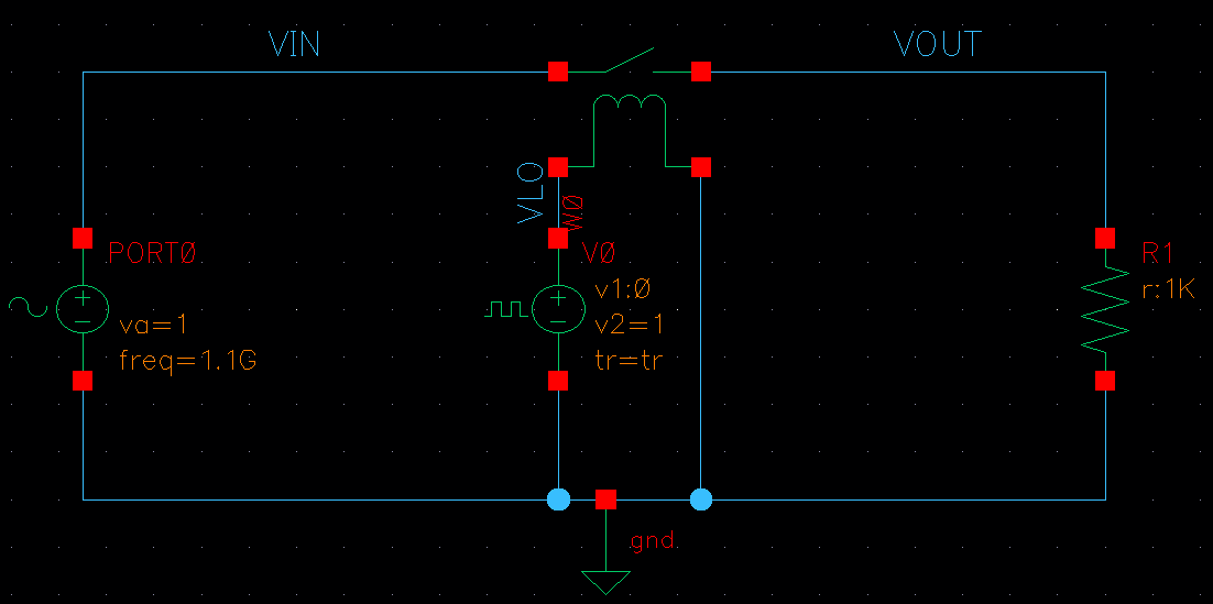
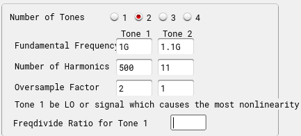
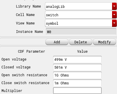
1.1.5 Simulation Verification of Switched Resistor Input Impedance
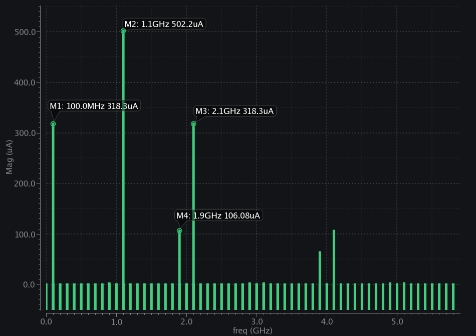
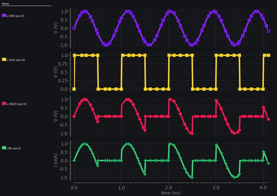
Images below show simulation verification of theory. We used 1k\(\Omega\) resistor, an ideal switch toggled at 1GHz CLK and excite the input with 1.1GHz sinusoid signal . Transient sim plots are shown. Purple being input, yellow CLK, red output voltage, and green input current. We also show input current spectrum. At input frequency of 1.1GHz, we see ~500uA current which means 2k\(\Omega\) resistance which matches with our expectation of \(R_{in}=2R\). We see at 100MHz i.e., \(\omega_{LO}-\omega_{IN}\) & at 2.1GHz i.e., \(\omega_{LO}+\omega_{IN}\) about 318uA current drawn which also matches with our expectation i.e. \(R_{in}=\pi R\) at these frequencies. Similarly, current at 1.9GHz i.e., \(3\omega_{LO}-\omega_{IN}\) is ~106uA which also matches with our expectation i.e. \(R_{in}=3\pi R\)
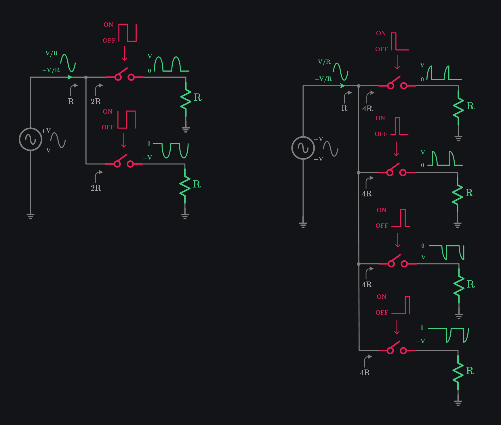
1.1.6 What if You Switched with Multi-Phase CLK
Say, now you use 0 and 180 deg CLK with 50% duty cycle and have schematic like in left figure. Or say, you have four phase CLK with 25% duty cycle and have a schematic like in right figure. What do you think the input current or impedance will look like? Input impedance will be just R, there is no transformation. From input side, current will be always drawn as if it is a continuous system (assuming ideal CLK and thus ignoring transitions). This is because when one switch turns OFF, other will turn ON, and input will continue to see load R all the time. It will look like R across the frequencies, and current drawn from input will be very clean i.e., a sinusoid current for sinusoid input voltage (unlike square current for sinusoid input for single phase CLK).
In other words, we can say all those resistors are seen in parallel even though they are never ON at same time!
1.1.7 Conversion Gain
You might ask what the significance of all this is? 1) You get to know how your impedance is scaled, so you can prepare your source for matching or driving the load; 2) You can easily compute gain from source to load, we call this “conversion gain” because now your load has multiple frequency components to it even though source was just one sinusoid, so you can “convert” how much signal is transferred from x frequency at input to y frequency at output.
Conversion gain has same scaling factor as impedance just that it is inversely related. So, at \(\omega_{IN}\), your impedance was scaled by 2, gain will be scaled by 1/2. At, \(\omega_{LO}\pm\omega_{IN}\), your impedance was scaled by \(\pi\), gain will be scaled by 1/\(\pi\), and so on…
The reason behind gain scaling is same as for impedance. We see the scaling because it is current that is actually getting scaled since we are not ON all the time. Current getting scaled down by factor x means:
- output voltage scaled down by factor x
- and effective impedance seen by input scaled up by factor x
1.1.8 Example
Say, you have 100\(\Omega\) load, switch resistance is 5\(\Omega\), source resistance is 50\(\Omega\)as shown in image below. Switch is driven by 50% duty cycle at \(\omega_{LO}\) frequency and input signal is at \(\omega_{IN}\) frequency with \(V_{IN}\) magnitude. What is the input resistance and conversion gain?

- Single Phase CLK: Current is scaled by Fourier coefficients of square wave, there output voltage is too. For example, current at \(\omega_{IN}\) is \(\frac{V_{IN}}{100+5+50}\) scaled by \(\frac{1}{2}\). This flows into physical 100\(\Omega\) load and develops \(\frac{100.V_{IN}}{2(100+5+50)}\), giving up conversion gain of \(\frac{100}{2(100+5+50)}\) at \(\omega_{IN}\). In other words, just do your regular voltage divider and then scale it by Fourier coefficient. Another interesting thing to note here is that since all the resistors in image above are in series, so they toggle ON/OFF together, i.e., when switch is ON, current flow and all resistors are seen, when switch is OFF, no current flows, nothing is seen, therefore input resistance is 2x of all the resistors (not just load resistor).
- Two Phase CLK: Input resistance is same across frequencies, therefore input current is clean sinusoid. However, as it passes through switches, it will again become square, therefore output will have similar “conversion gains” as in single phase CLK case. Input resistance is half compared to single phase case, therefore input current is doubled, but now “signal paths” are also doubled, therefore signal current to each individual phase remains as single phase giving us same gain. Also note that conversion gain measured between two phases differentially is doubled. How did signals become differential? LO signals impart their phases to output. If you switch something with 0 phase, output comes with 0+incoming signal phase. If you switch something with 180 phase, output comes with 180+incoming signal phase. Since incoming signal is common between two paths, therefore LO 0 and 180 phases are transferred to output and signal becomes differential. Also note, that avg value of LO waveform is same between 0 and 180 deg phases, therefore \(\omega_{IN}\) phase is not changed, and it gets cancelled. (Think of this way: \(\omega_{IN}\) multiplied with average value i.e., DC i.e., zero frequency and thus upconverted to same frequency)
1.2 When a Resistor is Switched ON & OFF with Current Source
So far, we’ve assumed a voltage source as the input. But what happens if we use a current source instead? After all, input impedance is a property of the circuit. It shouldn’t matter whether we excite the circuit with a voltage source or a current source, right? Right?
Well, now’s the time to read the fine print in textbooks.
This assumption does not hold for time-varying circuits. And switching, even simple on/off switching, introduces time variance. When the switch is ON, the circuit behaves one way. When it’s OFF, it behaves differently. You might think, “But I’m turning the switch on and off in a periodic and predictable way, like an LO continually turning ON and OFF mixer switches. So, does it still count as time-variant?” Yes. If the circuit’s output depends on absolute time, it is time-variant.
And in time-variant systems, the input impedance can change depending on whether you excite the circuit with a voltage source or a current source.
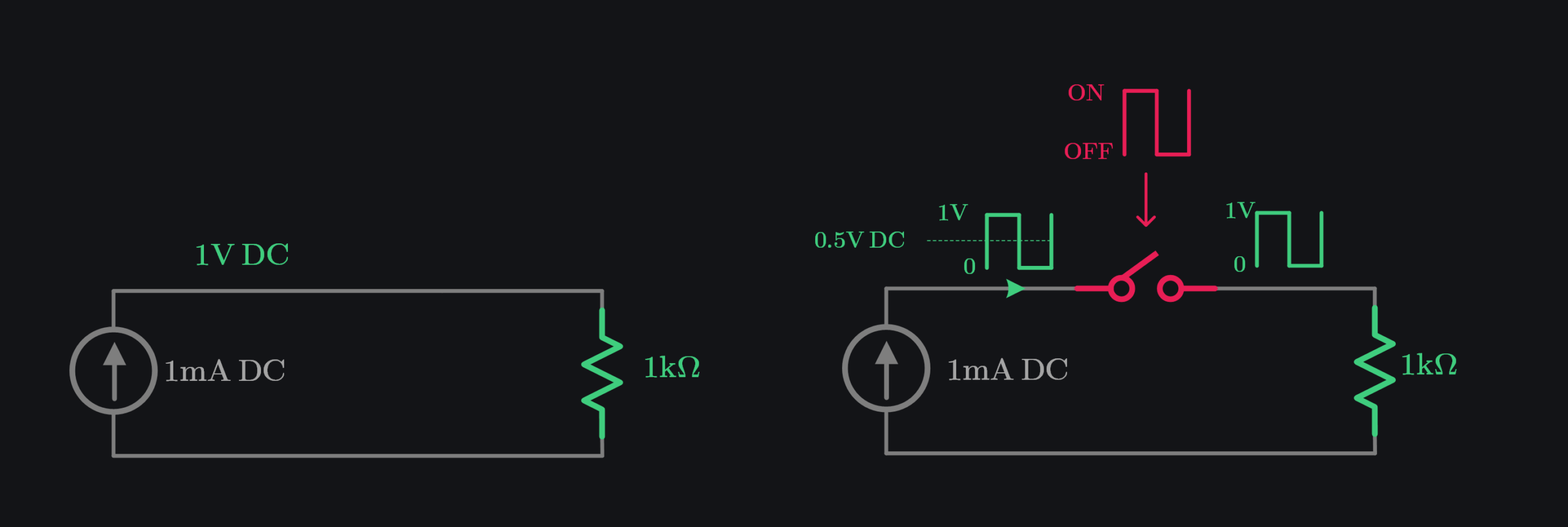
1.2.1 When Input is DC
Let’s repeat the same experiment as we did in 1.1.1 but now with current source. It turns out that scalars are flipped. Impedance which was \(2R\) in case of voltage source will look like \(\frac{R}{2} \) for current source. This makes sense because last time we said “Hey, this is as if half the current is drawn so impedance is doubled”, and now we can say, “Hey, this is as if half the voltage is developed so impedance is halved”
Note that when switch is OFF, current still needs a way to flow because it is a current source, we assume it flows into its own output impedance (not shown in image). We also assume output impedance is small, so that voltage developed is ~zero. If output impedance is big (which is actually true for a current source), it will develop huge voltage and dominate input impedance tainting our intuition. It would be absurd to drive a single phase with current source, so it’s not a realistic case, but we deal with it in example 1.2.3 anyway just to understand how we could analyze this. In reality, we have multi-phase CLK case, switch is always ON, taking current away from source impedance, and keeping voltage developed low.
1.2.2 General Formula
In general, for an input signal of frequency \(\omega_{IN}\) with 50% duty cycle driving a resistor R through a switch toggling at frequency \(\omega_{LO}\) and , we can write input resistance to be:
Note for a non-50 duty cycle, the Fourier coefficients can be calculated same was as explained in 1.1.4.
1.2.3 Example
Let’s take the same circuit as in example 1.1.8 and now excite it with current source and put source resistance in parallel. Let’s see how input resistance and conversion gains are impacted.

- Single Phase CLK: We see input resistance is scaled down by Fourier co-efficients whereas it was scaled up for voltage input case. Also note, input resistance toggles between \(R_{off}\) and \(R_{on}\) as shown in image (contrary to \(R_{on}\) and zero which we assumed in 1.2.1), therefore AVG resistance is \(\frac{1}{2}.(R_{off}-R_{on}) + R_{on}\), which is what we see at \(\omega_{IN}\).
- Two Phase CLK: Input resistance is fixed and same across frequencies, it does not toggle. We are measuring gain now in terms of transimpedance (output voltage over input current). It looks very similar to voltage gain case except for the fact that we multiply scalers (Fourier & current divider) with load impedance to come up with transimpedance value.
We are also attaching an excel calculator. Click on image below to download.

Does a capacitor behave in similar way when switched ON and OFF? Yes and No. Capacitor’s ability to hold voltage changes the game a bit and introduces what’s known as “Switched-cap resistor”. Let’s explore this in next chapter.
Browse by Tags
RFInsights
Published: 16 May 2025
Last Edit: 27 May 2025